- 您现在的位置:买卖IC网 > PDF目录8986 > AD5725ARSZ-500RL7 (Analog Devices Inc)IC DAC 12BIT QUAD PAR 28-SSOP PDF资料下载
参数资料
| 型号: | AD5725ARSZ-500RL7 |
| 厂商: | Analog Devices Inc |
| 文件页数: | 9/20页 |
| 文件大小: | 0K |
| 描述: | IC DAC 12BIT QUAD PAR 28-SSOP |
| 产品培训模块: | Data Converter Fundamentals DAC Architectures |
| 标准包装: | 1 |
| 设置时间: | 7µs |
| 位数: | 12 |
| 数据接口: | 并联 |
| 转换器数目: | 4 |
| 电压电源: | 双 ± |
| 功率耗散(最大): | 270mW |
| 工作温度: | -40°C ~ 85°C |
| 安装类型: | 表面贴装 |
| 封装/外壳: | 28-SSOP(0.209",5.30mm 宽) |
| 供应商设备封装: | 28-SSOP |
| 包装: | 标准包装 |
| 输出数目和类型: | 4 电压,单极;4 电压,双极 |
| 采样率(每秒): | * |
| 产品目录页面: | 784 (CN2011-ZH PDF) |
| 其它名称: | AD5725ARSZ-500RL7DKR |
Data Sheet
AD5725
Rev. C | Page 17 of 20
POWER SUPPLIES
Power supplies required are AVSS, AVDD, and VL. The AVSS
supply can be set between 15 V and 0 V. AVDD is the positive
supply; its operating range is between +5 V and +15 V.
VL is the digital output supply voltage for the readback function.
It is normally connected to +5 V. This pin is a logic reference
input only. It does not supply current to the device. If the readback
function is not used, VL can be left open-circuit. While VL does
not supply current to the AD5725, it does supply current to the
digital outputs when the readback function is used.
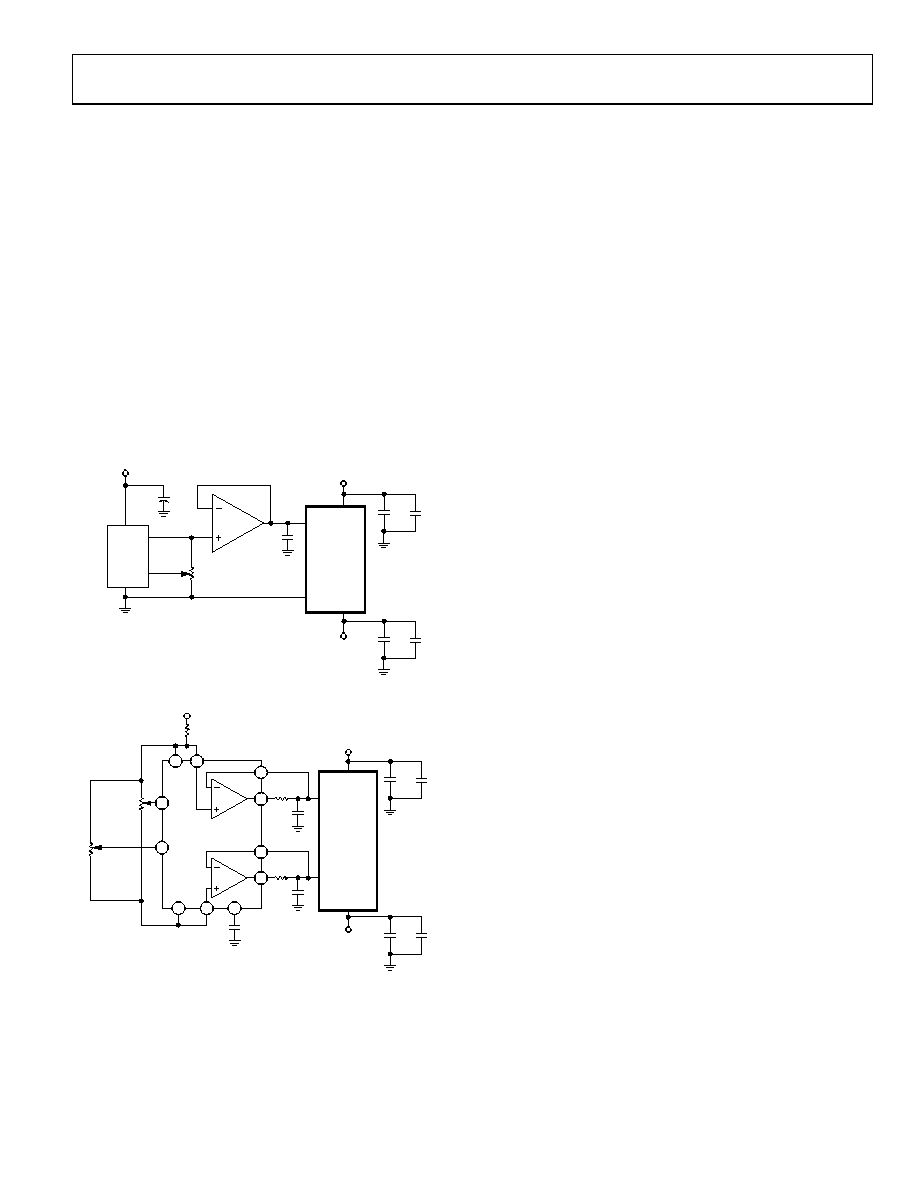
REFERENCE CONFIGURATION
Output voltage ranges can be configured as either unipolar or
bipolar, and within these choices, a wide variety of options
exists. The unipolar configuration can be either a positive or a
negative voltage output, and the bipolar configuration can be
either symmetrical or nonsymmetrical.
06442-
007
ADR01
+15V
INPUT
OUTPUT
TRIM
10k
+10V OPERATION
+15V
AD5725
–15V
OP1177
AVDD
AVSS
VREFP
0.2F
VREFN
+
10F
0.1F
10F
0.1F
Figure 27. Unipolar +10 V Operation
0.2F
AD5725
+15V
–15V
AVDD
VREFP
VREFN
AVSS
BALANCE
100k
GAIN
100kΩ
4
6
12
5
13
8
3
1
14
15
7
6.2Ω
0.2F
6.2Ω
1F
39kΩ
AD688 FOR ±10V
AD588 FOR ±5V
06442-
008
±5 OR ±10V OPERATION
10F
0.1F
10F
0.1F
Figure 28. Symmetrical Bipolar Operation
Figure 28 (Symmetrical Bipolar Operation) shows the AD5725
configured for ±10 V operation. See the AD688 data sheet for a
full explanation of reference operation. Adjustments may not be
required for many applications since the AD688 is a very high
accuracy reference. However, if additional adjustments are
required, adjust the AD5725 full scale first. Begin by loading the
digital full-scale code (0xFFF). Then, adjust the gain adjust
potentiometer to attain a DAC output voltage of 9.9976 V.
Then, adjust the balance adjust to set the mid-scale output
voltage to 0.000 V.
The 0.2 F bypass capacitors shown at the reference inputs in
Figure 28 should be used whenever ±10 V references are used.
Applications with single references or references to ±5 V may
not require the 0.2 F bypassing. The 6.2 Ω resistor in series
with the output of the reference amplifier is to keep the amplifier
from oscillating with the capacitive load. We have found that
this is large enough to stabilize this circuit. Larger resistor
values are acceptable, provided that the drop across the resistor
does not exceed a VBE. Assuming a minimum VBE of 0.6 V and a
maximum current of 2.75 mA, the resistor should be under
200 Ω for the loading of a single AD5725.
Using two separate references is not recommended. Having two
references can cause different drifts with time and temperature,
whereas with a single reference, most drifts will track.
Unipolar positive full-scale operation can usually be set with a
reference with the correct output voltage. This is preferable to
using a reference and dividing down to the required value. For a
10 V full-scale output, the circuit can be configured as shown in
Figure 29. In this configuration, the full-scale value is set first by
adjusting the 10 kΩ resistor for a full-scale output of 9.9976 V.
相关PDF资料 |
PDF描述 |
|---|---|
| VI-BNL-MV-F3 | CONVERTER MOD DC/DC 28V 150W |
| VI-BNL-MV-F2 | CONVERTER MOD DC/DC 28V 150W |
| VI-J44-MZ-F2 | CONVERTER MOD DC/DC 48V 25W |
| VI-BNL-MV-F1 | CONVERTER MOD DC/DC 28V 150W |
| DAC8043AFSZ | IC DAC 12BIT MULT SRL INP 8-SOIC |
相关代理商/技术参数 |
参数描述 |
|---|---|
| AD5725ARSZ-REEL | 功能描述:IC DAC 12BIT QUAD PAR 28-SSOP RoHS:是 类别:集成电路 (IC) >> 数据采集 - 数模转换器 系列:- 标准包装:47 系列:- 设置时间:2µs 位数:14 数据接口:并联 转换器数目:1 电压电源:单电源 功率耗散(最大):55µW 工作温度:-40°C ~ 85°C 安装类型:表面贴装 封装/外壳:28-SSOP(0.209",5.30mm 宽) 供应商设备封装:28-SSOP 包装:管件 输出数目和类型:1 电流,单极;1 电流,双极 采样率(每秒):* |
| AD5725BRSZ-1500RL7 | 功能描述:IC DAC 12BIT QUAD PAR 28-SSOP RoHS:是 类别:集成电路 (IC) >> 数据采集 - 数模转换器 系列:- 标准包装:1 系列:- 设置时间:4.5µs 位数:12 数据接口:串行,SPI? 转换器数目:1 电压电源:单电源 功率耗散(最大):- 工作温度:-40°C ~ 125°C 安装类型:表面贴装 封装/外壳:8-SOIC(0.154",3.90mm 宽) 供应商设备封装:8-SOICN 包装:剪切带 (CT) 输出数目和类型:1 电压,单极;1 电压,双极 采样率(每秒):* 其它名称:MCP4921T-E/SNCTMCP4921T-E/SNRCTMCP4921T-E/SNRCT-ND |
| AD5725BRSZ-1REEL | 功能描述:IC DAC 12BIT QUAD PAR 28-SSOP RoHS:是 类别:集成电路 (IC) >> 数据采集 - 数模转换器 系列:- 标准包装:47 系列:- 设置时间:2µs 位数:14 数据接口:并联 转换器数目:1 电压电源:单电源 功率耗散(最大):55µW 工作温度:-40°C ~ 85°C 安装类型:表面贴装 封装/外壳:28-SSOP(0.209",5.30mm 宽) 供应商设备封装:28-SSOP 包装:管件 输出数目和类型:1 电流,单极;1 电流,双极 采样率(每秒):* |
| AD5725BRSZ-500RL7 | 功能描述:IC DAC 12BIT QUAD PAR 28-SSOP RoHS:是 类别:集成电路 (IC) >> 数据采集 - 数模转换器 系列:- 标准包装:1 系列:- 设置时间:4.5µs 位数:12 数据接口:串行,SPI? 转换器数目:1 电压电源:单电源 功率耗散(最大):- 工作温度:-40°C ~ 125°C 安装类型:表面贴装 封装/外壳:8-SOIC(0.154",3.90mm 宽) 供应商设备封装:8-SOICN 包装:剪切带 (CT) 输出数目和类型:1 电压,单极;1 电压,双极 采样率(每秒):* 其它名称:MCP4921T-E/SNCTMCP4921T-E/SNRCTMCP4921T-E/SNRCT-ND |
| AD5725BRSZ-REEL | 功能描述:IC DAC 12BIT QUAD PAR 28-SSOP RoHS:是 类别:集成电路 (IC) >> 数据采集 - 数模转换器 系列:- 标准包装:47 系列:- 设置时间:2µs 位数:14 数据接口:并联 转换器数目:1 电压电源:单电源 功率耗散(最大):55µW 工作温度:-40°C ~ 85°C 安装类型:表面贴装 封装/外壳:28-SSOP(0.209",5.30mm 宽) 供应商设备封装:28-SSOP 包装:管件 输出数目和类型:1 电流,单极;1 电流,双极 采样率(每秒):* |
发布紧急采购,3分钟左右您将得到回复。