- 您现在的位置:买卖IC网 > PDF目录298813 > AD573AKD (ANALOG DEVICES INC) 1-CH 12-BIT SUCCESSIVE APPROXIMATION ADC, PARALLEL ACCESS, CDIP28 PDF资料下载
参数资料
| 型号: | AD573AKD |
| 厂商: | ANALOG DEVICES INC |
| 元件分类: | ADC |
| 英文描述: | 1-CH 12-BIT SUCCESSIVE APPROXIMATION ADC, PARALLEL ACCESS, CDIP28 |
| 封装: | HERMETIC SEALED, CERAMIC, DIP-28 |
| 文件页数: | 11/12页 |
| 文件大小: | 380K |
| 代理商: | AD573AKD |
AD574A
REV. B
–8–
The full-scale trim is done by applying a signal 1 1/2 LSB below
the nominal full scale (9.9963 for a 10 V range). Trim R2 to
give the last transition (1111 1111 1110 to 1111 1111 1111).
BIPOLAR OPERATION
The connections for bipolar ranges are shown in Figure 5.
Again, as for the unipolar ranges, if the offset and gain specifica-
tions are sufficient, one or both of the trimmers shown can be
replaced by a 50
± 1% fixed resistor. Bipolar calibration is
similar to unipolar calibration. First, a signal 1/2 LSB above
negative full scale (–4.9988 V for the
±5 V range) is applied and
R1 is trimmed to give the first transition (0000 0000 0000 to
0000 0000 0001). Then a signal 1 1/2 LSB below positive full
scale (+4.9963 V the
±5 V range) is applied and R2 trimmed to
give the last transition (1111 11111110 to 1111 1111 1111).
9
14
13
12
8
10
6
5
4
3
2
28
15
11
7
1
27
24
19
16
23
20
AD574A
STS
HIGH
BIT
MIDDLE
BITS
LOW
BITS
+5V
+15V
–15V
DIG COM
12/8
CS
AO
R/C
CE
REF IN
REF OUT
BIP OFF
10VIN
20VIN
ANA COM
GAIN
R2
100
ANALOG
INPUTS
5V
R1
100
10V
OFFSET
Figure 5. Bipolar Input Connections
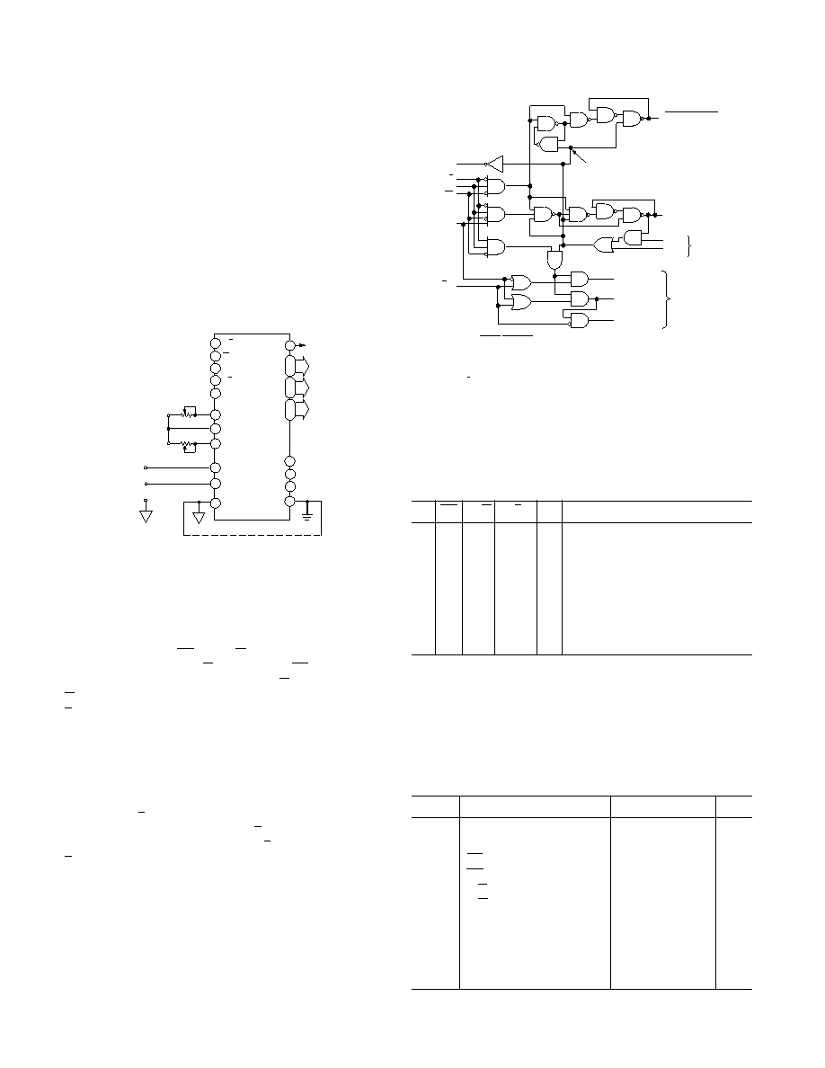
CONTROL LOGIC
The AD574A contains on-chip logic to provide conversion ini-
tiation and data read operations from signals commonly avail-
able in microprocessor systems. Figure 6 shows the internal
logic circuitry of the AD574A.
The control signals CE, CS, and R/C control the operation of
the converter. The state of R/C when CE and CS are both
asserted determines whether a data read (R/C = 1) or a convert
(R/C = 0) is in progress. The register control inputs AO and
12/8 control conversion length and data format. The AO line is
usually tied to the least significant bit of the address bus. If a
conversion is started with AO low, a full 12-bit conversion cycle
is initiated. If AO is high during a convert start, a shorter 8-bit
conversion cycle results. During data read operations, AO deter-
mines whether the three-state buffers containing the 8 MSBs of
the conversion result (AO = 0) or the 4 LSBs (AO = 1) are
enabled. The 12/8 pin determines whether the output data is
to be organized as two 8-bit words (12/8 tied to DIGITAL
COMMON) or a single 12-bit word (12/8 tied to VLOGIC). The
12/8 pin is not TTL-compatible and must be hard-wired to
either VLOGIC or DIGITAL COMMON. In the 8-bit mode, the
byte addressed when AO is high contains the 4 LSBs from the
conversion followed by four trailing zeroes. This organization
allows the data lines to be overlapped for direct interface to
8-bit buses without the need for external three-state buffers.
It is not recommended that AO change state during a data read
operation. Asymmetrical enable and disable times of the
three-state buffers could cause internal bus contention resulting
in potential damage to the AD574A.
READ
CONVERT
LOW IF CONVERSION
IN PROGRESS
VALUE OF A0
AT LAST CONVERT
COMMAND
EOC8
EOC12
FROM
NOTE 1
NIBBLE A, B,
ENABLE
NIBBLE C
ENABLE
NIBBLE B = O
ENABLE
TO OUTPUT
BUFFERS
START CONVERT
STATUS
R/C
CE
CS
A0
12/8
(NOTE 2)
NOTE 1: WHEN START CONVERT GOES LOW, THE EOC (END OF CONVERSION) SIGNALS GO LOW.
EOC8 RETURNS HIGH AFTER AN 8-BIT CONVERSION CYCLE IS COMPLETE, AND EOC12
RETURNS HIGH WHEN ALL 12-BITS HAVE BEEN CONVERTED. THE EOC SIGNALS PREVENT
DATA FROM BEING READ DURING CONVERSIONS.
NOTE 2: 12/8 IS NOT A TTL-COMPATABLE INPUT AND SHOULD ALWAYS BE WIRED DIRECTLY TO
VLOGIC OR DIGITAL COMMON.
Figure 6. AD574A Control Logic
An output signal, STS, indicates the status of the converter.
STS goes high at the beginning of a conversion and returns low
when the conversion cycle is complete.
Table I. AD574A Truth Table
CE CS
R/C 12/8
AO
Operation
0
X
None
X
1
X
None
1
0
X
0
Initiate 12-Bit Conversion
1
0
X
1
Initiate 8-Bit Conversion
1
0
1
Pin 1
X
Enable 12-Bit Parallel Output
1
0
1
Pin 15 0
Enable 8 Most Significant Bits
1
0
1
Pin 15 1
Enable 4 LSBs + 4 Trailing Zeroes
TIMING
The AD574A is easily interfaced to a wide variety of micropro-
cessors and other digital systems. The following discussion of
the timing requirements of the AD574A control signals should
provide the system designer with useful insight into the opera-
tion of the device.
Table II. Convert Start Timing—Full Control Mode
Symbol
Parameter
Min
Typ
Max
Units
tDSC
STS Delay from CE
400
ns
tHEC
CE Pulse Width
300
ns
tSSC
CS
to CE Setup
300
ns
tHSC
CS
Low During CE High
200
ns
tSRC
R/C to CE Setup
250
ns
tHRC
R/C Low During CE High
200
ns
tSAC
AO to CE Setup
0
ns
tHAC
AO Valid During CE High
300
ns
tC
Conversion Time
8-Bit Cycle
10
24
s
12-Bit Cycle
15
35
s
相关PDF资料 |
PDF描述 |
|---|---|
| AD573ALD | 1-CH 12-BIT SUCCESSIVE APPROXIMATION ADC, PARALLEL ACCESS, CDIP28 |
| AD573ASD | 1-CH 12-BIT SUCCESSIVE APPROXIMATION ADC, PARALLEL ACCESS, CDIP28 |
| AD6652XBC | SPECIALTY TELECOM CIRCUIT, PBGA256 |
| AD7575JP-REEL | 1-CH 8-BIT SUCCESSIVE APPROXIMATION ADC, PARALLEL ACCESS, PQCC20 |
| AD7575KP-REEL | 1-CH 8-BIT SUCCESSIVE APPROXIMATION ADC, PARALLEL ACCESS, PQCC20 |
相关代理商/技术参数 |
参数描述 |
|---|---|
| AD573JD | 功能描述:IC ADC 10BIT SAR REG 20-CDIP RoHS:否 类别:集成电路 (IC) >> 数据采集 - 模数转换器 系列:- 产品培训模块:Lead (SnPb) Finish for COTS Obsolescence Mitigation Program 标准包装:2,500 系列:- 位数:12 采样率(每秒):3M 数据接口:- 转换器数目:- 功率耗散(最大):- 电压电源:- 工作温度:- 安装类型:表面贴装 封装/外壳:SOT-23-6 供应商设备封装:SOT-23-6 包装:带卷 (TR) 输入数目和类型:- |
| AD573JN | 功能描述:IC ADC 10BIT SAR REGISTER 20-DIP RoHS:否 类别:集成电路 (IC) >> 数据采集 - 模数转换器 系列:- 标准包装:1 系列:- 位数:14 采样率(每秒):83k 数据接口:串行,并联 转换器数目:1 功率耗散(最大):95mW 电压电源:双 ± 工作温度:0°C ~ 70°C 安装类型:通孔 封装/外壳:28-DIP(0.600",15.24mm) 供应商设备封装:28-PDIP 包装:管件 输入数目和类型:1 个单端,双极 |
| AD573JNZ | 功能描述:IC ADC 10BIT SAR REGISTER 20-DIP RoHS:是 类别:集成电路 (IC) >> 数据采集 - 模数转换器 系列:- 标准包装:1 系列:microPOWER™ 位数:8 采样率(每秒):1M 数据接口:串行,SPI? 转换器数目:1 功率耗散(最大):- 电压电源:模拟和数字 工作温度:-40°C ~ 125°C 安装类型:表面贴装 封装/外壳:24-VFQFN 裸露焊盘 供应商设备封装:24-VQFN 裸露焊盘(4x4) 包装:Digi-Reel® 输入数目和类型:8 个单端,单极 产品目录页面:892 (CN2011-ZH PDF) 其它名称:296-25851-6 |
| AD573JP | 功能描述:IC ADC 10BIT SAR REGISTER 20PLCC RoHS:否 类别:集成电路 (IC) >> 数据采集 - 模数转换器 系列:- 标准包装:1 系列:- 位数:14 采样率(每秒):83k 数据接口:串行,并联 转换器数目:1 功率耗散(最大):95mW 电压电源:双 ± 工作温度:0°C ~ 70°C 安装类型:通孔 封装/外壳:28-DIP(0.600",15.24mm) 供应商设备封装:28-PDIP 包装:管件 输入数目和类型:1 个单端,双极 |
| AD573JPZ | 功能描述:IC ADC 10BIT SAR REGISTER 20PLCC RoHS:是 类别:集成电路 (IC) >> 数据采集 - 模数转换器 系列:- 标准包装:1 系列:- 位数:14 采样率(每秒):83k 数据接口:串行,并联 转换器数目:1 功率耗散(最大):95mW 电压电源:双 ± 工作温度:0°C ~ 70°C 安装类型:通孔 封装/外壳:28-DIP(0.600",15.24mm) 供应商设备封装:28-PDIP 包装:管件 输入数目和类型:1 个单端,双极 |
发布紧急采购,3分钟左右您将得到回复。