参数资料
| 型号: | AD5749ACPZ |
| 厂商: | Analog Devices Inc |
| 文件页数: | 17/28页 |
| 文件大小: | 0K |
| 描述: | IC CURRENT OUT DVR 32-LFCSP |
| 标准包装: | 1 |
| 放大器类型: | 仪表 |
| 电路数: | 1 |
| 电流 - 电源: | 5.2mA |
| 电流 - 输出 / 通道: | 24mA |
| 电压 - 电源,单路/双路(±): | 10.8 V ~ 55 V |
| 工作温度: | -40°C ~ 105°C |
| 安装类型: | 表面贴装 |
| 封装/外壳: | 32-VFQFN 裸露焊盘,CSP |
| 供应商设备封装: | 32-LFCSP-VQ(5x5) |
| 包装: | 托盘 |
第1页第2页第3页第4页第5页第6页第7页第8页第9页第10页第11页第12页第13页第14页第15页第16页当前第17页第18页第19页第20页第21页第22页第23页第24页第25页第26页第27页第28页
AD5749
Data Sheet
Rev. B | Page 24 of 28
APPLICATIONS INFORMATION
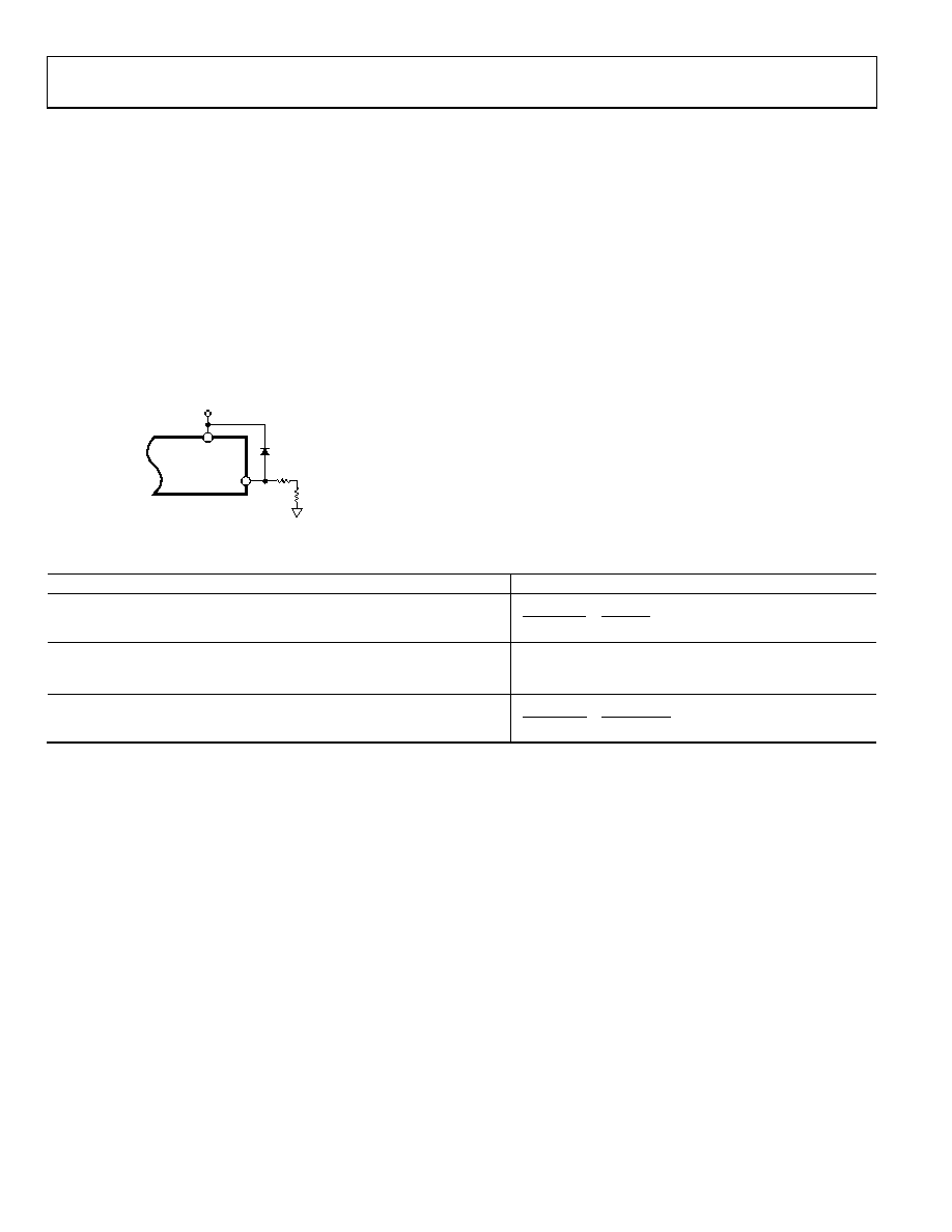
TRANSIENT VOLTAGE PROTECTION
The AD5749 contains ESD protection diodes that prevent damage
from normal handling. The industrial control environment can,
however, subject I/O circuits to much higher transients. To protect
the AD5749 from excessively high voltage transients, external
power diodes and a surge current limiting resistor may be
required, as shown in Figure 35. The constraint on the resistor
value is that during normal operation the output level at IOUT
must remain within its voltage compliance limit of AVDD
2.75 V and the two protection diodes and resistor must have
appropriate power ratings. Further protection can be added
with transient voltage suppressors if needed.
Figure 35. Output Transient Voltage Protection
THERMAL CONSIDERATIONS
It is important to understand the effects of power dissipation
on the package and how it affects junction temperature. The
internal junction temperature should not exceed 125°C. The
AD5749 is packaged in a 32-lead, 5 mm × 5 mm LFCSP pack-
age. The thermal impedance, θJA, is 42°C/W. It is important that
the devices not be operated under conditions that cause the
junction temperature to exceed its limit. Worst-case conditions
occur when the AD5749 is operated from the maximum AVDD
(55 V) and driving the maximum current (24 mA) directly to
ground. The quiescent current of the AD5749 should also be
taken into account, nominally ~4 mA.
The calculations in Table 12 estimate maximum power
dissipation under these worst-case conditions, and determine
maximum ambient temperature based on this. These figures
assume that proper layout and grounding techniques are
followed to minimize power dissipation, as outlined in the
Layout Guidelines section.
Table 12. Thermal and Supply Considerations
Considerations
32-Lead LFCSP Package
Maximum allowed power dissipation when operating at an ambient
temperature of 85°C
W
95
.
0
42
85
125
=
=
JA
A
JMAX
θ
T
Maximum allowed ambient temperature when operating from a supply of
55 V and driving 24 mA directly to ground (include 4 mA for internal AD5749
current)
TJMAX (PD × θJA) = 125 ((55 × 0.028) × 42) = 60.3°C
Maximum allowed supply voltage when operating at an ambient
temperature of 85°C and driving 24 mA directly to ground
(
)
V
34
42
028
.
0
85
125
=
×
=
×
JA
DD
A
JMAX
θ
AI
T
AD5749
08923-
036
AVDD
IOUT
RP
RLOAD
相关PDF资料 |
PDF描述 |
|---|---|
| AD5750-1ACPZ-REEL7 | IC CURR/VOLT OUT DVR 32LFCSP |
| AD5750-2BCPZ-RL7 | IC CURR/VOLT OUT DRVR 32LFCSP |
| AD5751ACPZ-REEL7 | IC I/V OUTPUT DRIVER 60V 32LFCSP |
| AD582SD | IC AMP SAMPLE HOLD 25MA 14CDIP |
| AD585SQ | IC AMP SAMPLE HOLD 50MA 14CDIP |
相关代理商/技术参数 |
参数描述 |
|---|---|
| AD5749ACPZ-RL7 | 功能描述:IC CURRENT OUT DVR 32-LFCSP RoHS:是 类别:集成电路 (IC) >> Linear - Amplifiers - Instrumentation 系列:- 标准包装:50 系列:LinCMOS™ 放大器类型:通用 电路数:4 输出类型:- 转换速率:0.05 V/µs 增益带宽积:110kHz -3db带宽:- 电流 - 输入偏压:0.7pA 电压 - 输入偏移:210µV 电流 - 电源:57µA 电流 - 输出 / 通道:30mA 电压 - 电源,单路/双路(±):3 V ~ 16 V,±1.5 V ~ 8 V 工作温度:-40°C ~ 85°C 安装类型:表面贴装 封装/外壳:14-SOIC(0.154",3.90mm 宽) 供应商设备封装:14-SOIC 包装:管件 产品目录页面:865 (CN2011-ZH PDF) 其它名称:296-1834296-1834-5 |
| AD574A | 制造商:AD 制造商全称:Analog Devices 功能描述:Complete 12-Bit A/D Converter |
| AD574AJ | 制造商:AD 制造商全称:Analog Devices 功能描述:Complete 12-Bit A/D Converter |
| AD574AJD | 功能描述:IC ADC 12BIT W/REF 28-CDIP RoHS:否 类别:集成电路 (IC) >> 数据采集 - 模数转换器 系列:- 标准包装:1 系列:- 位数:14 采样率(每秒):83k 数据接口:串行,并联 转换器数目:1 功率耗散(最大):95mW 电压电源:双 ± 工作温度:0°C ~ 70°C 安装类型:通孔 封装/外壳:28-DIP(0.600",15.24mm) 供应商设备封装:28-PDIP 包装:管件 输入数目和类型:1 个单端,双极 |
发布紧急采购,3分钟左右您将得到回复。