- 您现在的位置:买卖IC网 > PDF目录10516 > AD574AKD (Analog Devices Inc)IC ADC 12BIT W/REF 28-CDIP PDF资料下载
参数资料
| 型号: | AD574AKD |
| 厂商: | Analog Devices Inc |
| 文件页数: | 3/12页 |
| 文件大小: | 0K |
| 描述: | IC ADC 12BIT W/REF 28-CDIP |
| 标准包装: | 1 |
| 位数: | 12 |
| 采样率(每秒): | 28.6k |
| 数据接口: | 并联 |
| 转换器数目: | 1 |
| 功率耗散(最大): | 725mW |
| 电压电源: | 双 ± |
| 工作温度: | 0°C ~ 70°C |
| 安装类型: | 通孔 |
| 封装/外壳: | 28-CDIP(0.605",15.37mm) |
| 供应商设备封装: | 28-CDIP |
| 包装: | 管件 |
| 输入数目和类型: | 2 个单端,单极;2 个单端,双极 |
| 产品目录页面: | 777 (CN2011-ZH PDF) |
AD574A
REV. B
–11–
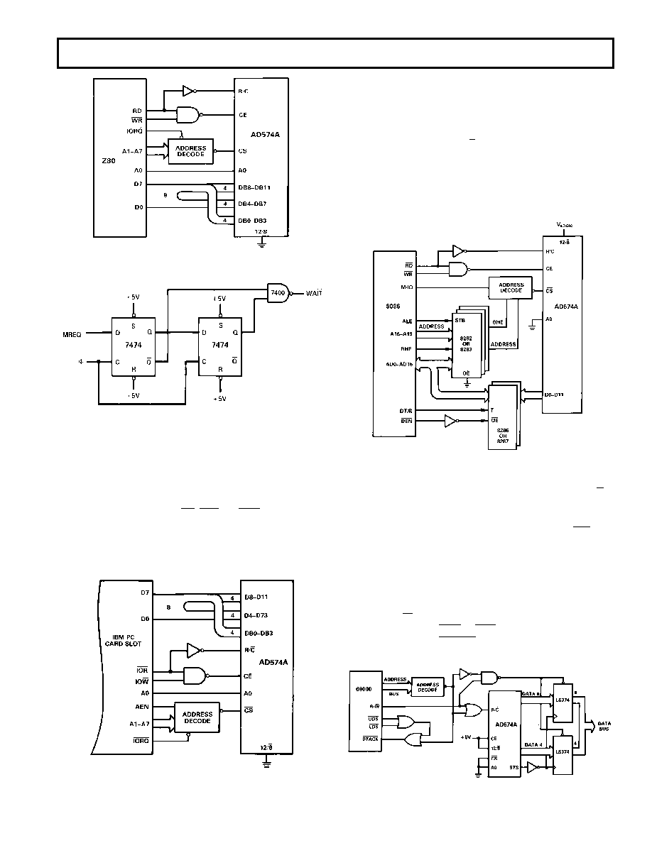
Figure 15. Z80—AD574A Interface
Figure 16. Wait State Generator
IBM PC Interface
The AD574A appears in Figure 17 interfaced to the 4 MHz
8088 processor of an IBM PC. Since the device resides in I/O
space, its address is decoded from only the lower ten address
lines and must be gated with AEN (active low) to mask out in-
ternal DMA cycles which use the same I/O address space. This
active low signal is applied to CS. IOR and IOW are used to
initiate the conversion and read, and are gated together to drive
the chip enable, CE. Because the data bus width is limited to
8 bits, the AD574A data resides in two adjacent addresses
selected by A0.
Figure 17. IBM PC—AD574A Interface
Note: Due to the large number of options that may be installed
in the PC, the I/O bus loading should be limited to one Schottky
TTL load. Therefore, a buffer/driver should be used when inter-
facing more than two AD574As to the I/O bus.
8086 Interface
The data mode select pin (12/8) of the AD574A should be con-
nected to VLOGIC to provide a 12-bit data output. To prevent
possible bus contention, a demultiplexed and buffered address/
data bus is recommended. In the cases where the 8-bit short
conversion cycle is not used, A0 should be tied to digital com-
mon. Figure 18 shows a typical 8086 configuration.
Figure 18. 8086—AD574A with Buffered Bus lnterface
For clock speeds greater than 4 MHz wait state insertion similar
to Figure 16 is recommended to ensure sufficient CE and R/C
pulse duration.
The AD574A can also be interfaced in a stand-alone mode (see
Figure 13). A low going pulse derived from the 8086’s WR sig-
nal logically ORed with a low address decode starts the conver-
sion. At the end of the conversion, STS clocks the data into the
three-state latches.
68000 Interface
The AD574, when configured in the stand-alone mode, will eas-
ily interface to the 4 MHz version of the 68000 microprocessor.
The 68000 R/W signal combined with a low address decode ini-
tiates conversion. The UDS or LDS signal, with the decoded
address, generates the DTACK input to the processor, latching
in the AD574A’s data. Figure 19 illustrates this configuration.
Figure 19. 68000—AD574A Interface
相关PDF资料 |
PDF描述 |
|---|---|
| UP050B910K-KFC | CAP CER 91PF 50V 10% AXIAL |
| VE-B4H-MW | CONVERTER MOD DC/DC 52V 100W |
| AD9251BCPZ-80 | IC ADC 14BIT 80MSPS 64LFCSP |
| VE-B4F-MX-F4 | CONVERTER MOD DC/DC 72V 75W |
| MAX13020ASA+ | IC TRANSCEIVER LIN 8-SOIC |
相关代理商/技术参数 |
参数描述 |
|---|---|
| AD574AKD/+ | 制造商:Analog Devices 功能描述: |
| AD574AKE | 功能描述:IC ADC 12BIT W/REF/CLK 28-CLCC RoHS:否 类别:集成电路 (IC) >> 数据采集 - 模数转换器 系列:- 产品培训模块:Lead (SnPb) Finish for COTS Obsolescence Mitigation Program 标准包装:2,500 系列:- 位数:12 采样率(每秒):3M 数据接口:- 转换器数目:- 功率耗散(最大):- 电压电源:- 工作温度:- 安装类型:表面贴装 封装/外壳:SOT-23-6 供应商设备封装:SOT-23-6 包装:带卷 (TR) 输入数目和类型:- |
| AD574AKE/+ | 制造商:Rochester Electronics LLC 功能描述:- Bulk |
| AD574AKN | 功能描述:IC ADC 12BIT W/REF 28-DIP RoHS:否 类别:集成电路 (IC) >> 数据采集 - 模数转换器 系列:- 标准包装:1 系列:- 位数:14 采样率(每秒):83k 数据接口:串行,并联 转换器数目:1 功率耗散(最大):95mW 电压电源:双 ± 工作温度:0°C ~ 70°C 安装类型:通孔 封装/外壳:28-DIP(0.600",15.24mm) 供应商设备封装:28-PDIP 包装:管件 输入数目和类型:1 个单端,双极 |
| AD574AKN/+ | 制造商:Analog Devices 功能描述:ADC SGL SAR 12-BIT PARALLEL 28PDIP W - Rail/Tube 制造商:Rochester Electronics LLC 功能描述:IC, MONO 12-BIT A/D CONV. - Bulk |
发布紧急采购,3分钟左右您将得到回复。