- 您现在的位置:买卖IC网 > PDF目录10062 > AD574AKP (Analog Devices Inc)IC ADC 12BIT W/REF/CLK 28-PLCC PDF资料下载
参数资料
| 型号: | AD574AKP |
| 厂商: | Analog Devices Inc |
| 文件页数: | 9/12页 |
| 文件大小: | 0K |
| 描述: | IC ADC 12BIT W/REF/CLK 28-PLCC |
| 标准包装: | 1 |
| 位数: | 12 |
| 采样率(每秒): | 28.6k |
| 数据接口: | 并联 |
| 转换器数目: | 1 |
| 功率耗散(最大): | 725mW |
| 电压电源: | 双 ± |
| 工作温度: | 0°C ~ 70°C |
| 安装类型: | 表面贴装 |
| 封装/外壳: | 28-LCC(J 形引线) |
| 供应商设备封装: | 28-PLCC(11.51x11.51) |
| 包装: | 管件 |
| 输入数目和类型: | 2 个单端,单极;2 个单端,双极 |
AD574A
REV. B
–6–
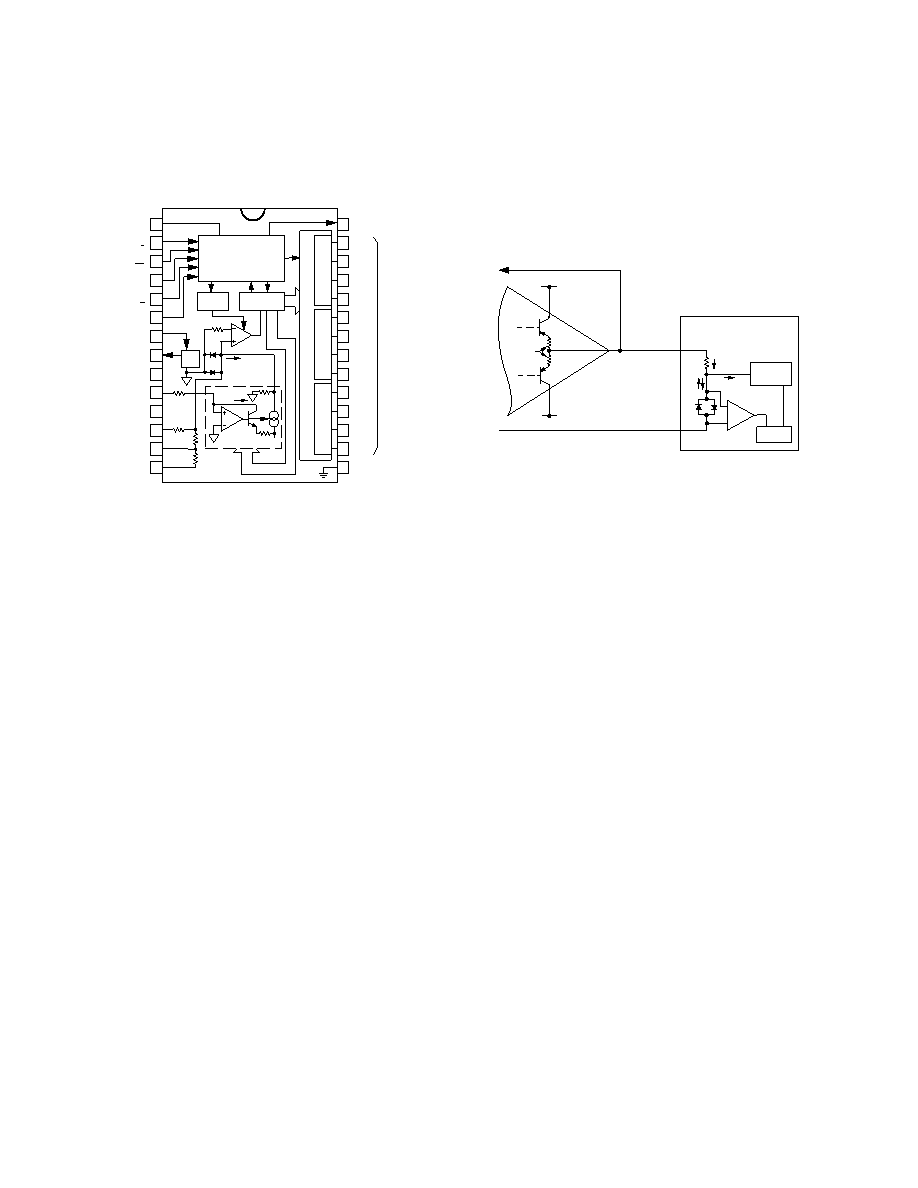
CIRCUIT OPERATION
The AD574A is a complete 12-bit A/D converter which requires
no external components to provide the complete successive-
approximation analog-to-digital conversion function. A block
diagram of the AD574A is shown in Figure 1.
1
14
28
15
2
3
4
5
6
7
8
9
10
11
12
13
27
26
25
24
23
22
21
20
19
18
17
16
CONTROL
CLOCK
SAR
3
S
T
A
T
E
O
U
T
P
U
T
B
U
F
E
R
S
MSB
N
I
B
L
E
N
I
B
L
E
N
I
B
L
E
LSB
10V
REF
12
C
B
A
12
AD574A
3k
19.95k
9.95k
5k
N
DAC
VEE
8k
IREF
COMP
DIGITAL COMMON
DC
IDAC
IDAC =
4 x N x IREF
+5V SUPPLY
VLOGIC
DATA MODE SELECT
12/8
STATUS
STS
DB11
MSB
DB10
DB9
DB8
DB7
DB6
DB5
DB4
DB3
DB2
DB1
DB0
LSB
DIGITAL
DATA
OUTPUTS
CHIP SELECT
CS
BYTE ADDRESS/
SHORT CYCLE
AO
READ/CONVERT
R/C
CHIP ENABLE
CE
+12/+15V SUPPLY
VCC
+10V REFERENCE
REF OUT
ANALOG COMMON
AC
REFERENCE INPUT
REF IN
-12/-15V SUPPLY
VEE
BIPOLAR OFFSET
BIP OFF
10V SPAN INPUT
10VIN
20V SPAN INPUT
20VIN
Figure 1. Block Diagram of AD574A 12-Bit A-to-D Converter
When the control section is commanded to initiate a conversion
(as described later), it enables the clock and resets the successive-
approximation register (SAR) to all zeros. Once a conversion
cycle has begun, it cannot be stopped or restarted and data is
not available from the output buffers. The SAR, timed by the
clock, will sequence through the conversion cycle and return an
end-of-convert flag to the control section. The control section
will then disable the clock, bring the output status flag low, and
enable control functions to allow data read functions by external
command.
During the conversion cycle, the internal 12-bit current output
DAC is sequenced by the SAR from the most significant bit
(MSB) to least significant bit (LSB) to provide an output cur-
rent which accurately balances the input signal current through
the 5 k
(or 10 k) input resistor. The comparator determines
whether the addition of each successively-weighted bit current
causes the DAC current sum to be greater or less than the input
current; if the sum is less, the bit is left on; if more, the bit is
turned off. After testing all the bits, the SAR contains a 12-bit
binary code which accurately represents the input signal to
within
±1/2 LSB.
The temperature-compensated buried Zener reference provides
the primary voltage reference to the DAC and guarantees excel-
lent stability with both time and temperature. The reference is
trimmed to 10.00 volts
±0.2%; it can supply up to 1.5 mA to an
external load in addition to the requirements of the reference in-
put resistor (0.5 mA) and bipolar offset resistor (1 mA) when
the AD574A is powered from
±15 V supplies. If the AD574A is
used with
±12 V supplies, or if external current must be sup-
plied over the full temperature range, an external buffer ampli-
fier is recommended. Any external load on the AD574A
reference must remain constant during conversion. The
thin-film application resistors are trimmed to match the
full-scale output current of the DAC. There are two 5 k
input
scaling resistors to allow either a 10 volt or 20 volt span. The
10 k
bipolar offset resistor is grounded for unipolar operation
and connected to the 10 volt reference for bipolar operation.
DRIVING THE AD574 ANALOG INPUT
The internal circuitry of the AD574 dictates that its analog
input be driven by a low source impedance. Voltage changes at
the current summing node of the internal comparator result in
abrupt modulations of the current at the analog input. For accu-
rate 12-bit conversions the driving source must be capable of
holding a constant output voltage under these dynamically
changing load conditions.
CURRENT
OUTPUT
DAC
SAR
COMPARATOR
AD574A
IIN
iTEST
RIN
iDIFF
V+
V–
FEEDBACK TO AMPLIFIER
ANALOG COMMON
I
IN IS MODULATED BY
CHANGES IN TEST CURRENT.
AMPLIFIER PULSE LOAD
RESPONSE LIMITED BY
OPEN LOOP OUTPUT IMPEDANCE.
CURRENT
LIMITING
RESISTORS
Figure 2. Op Amp – AD574A Interface
The output impedance of an op amp has an open-loop value
which, in a closed loop, is divided by the loop gain available at
the frequency of interest. The amplifier should have acceptable
loop gain at 500 kHz for use with the AD574A. To check
whether the output properties of a signal source are suitable,
monitor the AD574’s input with an oscilloscope while a conver-
sion is in progress. Each of the 12 disturbances should subside
in 1
s or less.
For applications involving the use of a sample-and-hold ampli-
fier, the AD585 is recommended. The AD711 or AD544 op
amps are recommended for dc applications.
SAMPLE-AND-HOLD AMPLIFIERS
Although the conversion time of the AD574A is a maximum of
35
s, to achieve accurate 12-bit conversions of frequencies
greater than a few Hz requires the use of a sample-and-hold
amplifier (SHA). If the voltage of the analog input signal driving
the AD574A changes by more than 1/2 LSB over the time
interval needed to make a conversion, then the input requires a
SHA.
The AD585 is a high linearity SHA capable of directly driving
the analog input of the AD574A. The AD585’s fast acquisition
time, low aperture and low aperture jitter are ideally suited for
high-speed data acquisition systems. Consider the AD574A
converter with a 35
s conversion time and an input signal of
10 V p-p: the maximum frequency which may be applied to
achieve rated accuracy is 1.5 Hz. However, with the addition of
an AD585, as shown in Figure 3, the maximum frequency
increases to 26 kHz.
The AD585’s low output impedance, fast-loop response, and
low droop maintain 12-bits of accuracy under the changing load
conditions that occur during a conversion, making it suitable for
use in high accuracy conversion systems. Many other SHAs
cannot achieve 12-bits of accuracy and can thus compromise a
system. The AD585 is recommended for AD574A applications
requiring a sample and hold.
An alternate approach is to use the AD1674, which combines
the ADC and SHA on one chip, with a total throughput time of
10
s.
相关PDF资料 |
PDF描述 |
|---|---|
| MS27484T16B26PD | CONN PLUG 26POS STRAIGHT W/PINS |
| LTC2206IUK-14#TRPBF | IC ADC 14-BIT 80MSPS 48-QFN |
| VE-J04-MX-S | CONVERTER MOD DC/DC 48V 75W |
| VI-B6L-MW-F3 | CONVERTER MOD DC/DC 28V 100W |
| VE-J03-MX-S | CONVERTER MOD DC/DC 24V 75W |
相关代理商/技术参数 |
参数描述 |
|---|---|
| AD574AKP-REEL | 功能描述:IC ADC 12BIT W/REF/CLK 28-PLCC RoHS:否 类别:集成电路 (IC) >> 数据采集 - 模数转换器 系列:- 标准包装:1 系列:- 位数:14 采样率(每秒):83k 数据接口:串行,并联 转换器数目:1 功率耗散(最大):95mW 电压电源:双 ± 工作温度:0°C ~ 70°C 安装类型:通孔 封装/外壳:28-DIP(0.600",15.24mm) 供应商设备封装:28-PDIP 包装:管件 输入数目和类型:1 个单端,双极 |
| AD574AKPZ | 功能描述:IC ADC 12BIT W/REF/CLK 28-PLCC RoHS:是 类别:集成电路 (IC) >> 数据采集 - 模数转换器 系列:- 其它有关文件:TSA1204 View All Specifications 标准包装:1 系列:- 位数:12 采样率(每秒):20M 数据接口:并联 转换器数目:2 功率耗散(最大):155mW 电压电源:模拟和数字 工作温度:-40°C ~ 85°C 安装类型:表面贴装 封装/外壳:48-TQFP 供应商设备封装:48-TQFP(7x7) 包装:Digi-Reel® 输入数目和类型:4 个单端,单极;2 个差分,单极 产品目录页面:1156 (CN2011-ZH PDF) 其它名称:497-5435-6 |
| AD574AKPZ-REEL | 功能描述:IC ADC 12BIT W/REF/CLK 28-PLCC RoHS:是 类别:集成电路 (IC) >> 数据采集 - 模数转换器 系列:- 产品培训模块:Lead (SnPb) Finish for COTS Obsolescence Mitigation Program 标准包装:2,500 系列:- 位数:12 采样率(每秒):3M 数据接口:- 转换器数目:- 功率耗散(最大):- 电压电源:- 工作温度:- 安装类型:表面贴装 封装/外壳:SOT-23-6 供应商设备封装:SOT-23-6 包装:带卷 (TR) 输入数目和类型:- |
| AD574AKX | 制造商:AD 制造商全称:Analog Devices 功能描述:Complete 12-Bit A/D Converter |
| AD574AL | 制造商:AD 制造商全称:Analog Devices 功能描述:Complete 12-Bit A/D Converter |
发布紧急采购,3分钟左右您将得到回复。