参数资料
| 型号: | AD5780BCPZ |
| 厂商: | Analog Devices Inc |
| 文件页数: | 27/28页 |
| 文件大小: | 0K |
| 描述: | IC DAC VOLT OUT 18BIT 24LFCSP |
| 标准包装: | 1 |
| 设置时间: | 2.5µs |
| 位数: | 18 |
| 数据接口: | DSP,MICROWIRE?,QSPI?,串行,SPI? |
| 转换器数目: | 1 |
| 电压电源: | 模拟和数字,双 ± |
| 工作温度: | -40°C ~ 125°C |
| 安装类型: | 表面贴装 |
| 封装/外壳: | 24-VFQFN 裸露焊盘,CSP |
| 供应商设备封装: | 24-LFCSP-VQ EP(4x5) |
| 包装: | 托盘 |
| 输出数目和类型: | 1 电压,双极 |
第1页第2页第3页第4页第5页第6页第7页第8页第9页第10页第11页第12页第13页第14页第15页第16页第17页第18页第19页第20页第21页第22页第23页第24页第25页第26页当前第27页第28页
AD5780
Data Sheet
Rev. E | Page 8 of 28
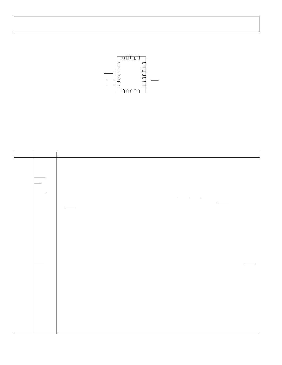
PIN CONFIGURATION AND FUNCTION DESCRIPTIONS
2
1
3
4
5
6
7
18
19
17
16
15
14
13
LDAC
CLR
VDD
RESET
VDD
VREFP
VOUT
SCLK
SYNC
DGND
VREFN
VSS
AGND
NOTES
1. DNC = DO NOT CONNECT. DO NOT CONNECT TO THIS PIN.
2. NEGATIVE ANALOG SUPPLY CONNECTION (VSS).
A VOLTAGE IN THE RANGE OF –16.5 V TO –2.5 V
CAN BE CONNECTED. VSS SHOULD BE DECOUPLED
TO AGND. THE PADDLE CAN BE LEFT ELECTRICALLY
UNCONNECTED PROVIDED THAT A SUPPLY
CONNECTION IS MADE AT THE VSS PINS. IT IS
RECOMMENDED THAT THE PADDLE BE THERMALLY
CONNECTED TO A COPPER PLANE FOR ENHANCED
THERMAL PERFORMANCE.
9
1
0
1
2
8
IO
V
C
D
N
C
S
D
O
S
D
IN
V
C
AD5780
TOP VIEW
(Not to Scale)
2
1
2
0
2
D
N
C
R
F
B
D
N
C
2
3
D
N
C
2
4
IN
V
0
964
9-
00
5
Figure 4. Pin Configuration
Table 5. Pin Function Descriptions
Pin No.
Mnemonic
Description
1
VOUT
Analog Output Voltage.
2
VREFP
Positive Reference Voltage Input. A voltage in the range of 5 V to VDD 2.5 V can be connected to this pin.
3, 5
VDD
Positive Analog Supply Connection. A voltage in the range of 7.5 V to 16.5 V can be connected to this pin. VDD must
be decoupled to AGND.
4
RESET
Active Low Reset. Asserting this pin returns the AD5780 to its power-on status.
6
CLR
Active Low Input. Asserting this pin sets the DAC register to a user defined value (see Table 12) and updates the DAC
output. The output value depends on the DAC register coding that is being used, either binary or twos complement.
7
LDAC
Active Low Load DAC Logic Input. This pin is used to update the DAC register and, consequently, the analog output.
When tied permanently low, the output is updated on the rising edge of SYNC. If LDAC is held high during the write
cycle, the input register is updated, but the output update is held off until the falling edge of LDAC. Do not leave
the LDAC pin unconnected.
8
VCC
Digital Supply. Voltage range is from 2.7 V to 5.5 V. VCC should be decoupled to DGND.
9
IOVCC
Digital Interface Supply. Digital threshold levels are referenced to the voltage applied to this pin. Voltage range is
from 1.71 V to 5.5 V.
10, 21,
22, 23
DNC
Do Not Connect. Do not connect to these pins.
11
SDO
Serial Data Output. Data is clocked out on the rising edge of the serial clock input.
12
SDIN
Serial Data Input. This device has a 24-bit input shift register. Data is clocked into the register on the falling edge of
the serial clock input.
13
SCLK
Serial Clock Input. Data is clocked into the input shift register on the falling edge of the serial clock input. Data can
be transferred at rates of up to 35 MHz.
14
SYNC
Level Triggered Control Input (Active Low). This is the frame synchronization signal for the input data. When SYNC
goes low, it enables the input shift register, and data is then transferred in on the falling edges of the following
clocks. The DAC is updated on the rising edge of SYNC.
15
DGND
Ground Reference Pin for Digital Circuitry.
16
VREFN
Negative Reference Voltage Input.
17, 18
VSS
Negative Analog Supply Connection. A voltage in the range of 16.5 V to 2.5 V can be connected to this pin.
VSS must be decoupled to AGND.
19
AGND
Ground Reference Pin for Analog Circuitry.
20
RFB
Feedback Connection for External Amplifier. See the AD5780 Features section for further details.
24
INV
Inverting Input Connection for External Amplifier. See the AD5780 Features section for further details.
EPAD
VSS
Negative Analog Supply Connection (VSS). A voltage in the range of 16.5 V to 2.5 V can be connected to this pin.
VSS must be decoupled to AGND. The paddle can be left electrically unconnected provided that a supply connection is
made at the VSS pins. It is recommended that the paddle be thermally connected to a copper plane for enhanced
thermal performance.
相关PDF资料 |
PDF描述 |
|---|---|
| AD5930YRUZ-REEL7 | IC GEN PROG FREQ BURST 20TSSOP |
| AD5932YRUZ-REEL7 | IC PROG WAVEFORM GENERAT 16TSSOP |
| AD5933YRSZ-REEL7 | NETWORK ANALYZER 12B 1MSP 16SSOP |
| AD5934YRSZ | IC NTWK ANALYZER 12B 1MSP 16SSOP |
| AD598JR | IC LVDT SGNL COND OSC/REF 20SOIC |
相关代理商/技术参数 |
参数描述 |
|---|---|
| AD5780BCPZ-REEL7 | 制造商:Analog Devices 功能描述:DAC 1-CH Segment 18-bit 24-Pin LFCSP EP T/R 制造商:Analog Devices 功能描述:18BIT, 1LSB, BUFFERED REF - Tape and Reel 制造商:Analog Devices 功能描述:IC DAC VOLT OUT 18BIT 24LFCSP 制造商:Analog Devices Inc. 功能描述:Digital to Analog Converters - DAC 18bit 1LSB buffered Ref 制造商:Analog Devices 功能描述:CONVERTER - DAC |
| AD5781 | 制造商:AD 制造商全称:Analog Devices 功能描述:Ultra Stable, 16-Bit ±0.5 LSB INL |
| AD5781ARUZ | 功能描述:IC DAC 18BIT SRL 20TSSOP RoHS:是 类别:集成电路 (IC) >> 数据采集 - 数模转换器 系列:- 标准包装:1 系列:- 设置时间:4.5µs 位数:12 数据接口:串行,SPI? 转换器数目:1 电压电源:单电源 功率耗散(最大):- 工作温度:-40°C ~ 125°C 安装类型:表面贴装 封装/外壳:8-SOIC(0.154",3.90mm 宽) 供应商设备封装:8-SOICN 包装:剪切带 (CT) 输出数目和类型:1 电压,单极;1 电压,双极 采样率(每秒):* 其它名称:MCP4921T-E/SNCTMCP4921T-E/SNRCTMCP4921T-E/SNRCT-ND |
| AD5781ARUZ-REEL7 | 功能描述:IC DAC 18BIT SRL 20TSSOP RoHS:是 类别:集成电路 (IC) >> 数据采集 - 数模转换器 系列:- 产品培训模块:Data Converter Fundamentals DAC Architectures 标准包装:750 系列:- 设置时间:7µs 位数:16 数据接口:并联 转换器数目:1 电压电源:双 ± 功率耗散(最大):100mW 工作温度:0°C ~ 70°C 安装类型:表面贴装 封装/外壳:28-LCC(J 形引线) 供应商设备封装:28-PLCC(11.51x11.51) 包装:带卷 (TR) 输出数目和类型:1 电压,单极;1 电压,双极 采样率(每秒):143k |
| AD5781BRUZ | 功能描述:IC DAC 18BIT SRL 20TSSOP RoHS:是 类别:集成电路 (IC) >> 数据采集 - 数模转换器 系列:- 标准包装:1 系列:- 设置时间:4.5µs 位数:12 数据接口:串行,SPI? 转换器数目:1 电压电源:单电源 功率耗散(最大):- 工作温度:-40°C ~ 125°C 安装类型:表面贴装 封装/外壳:8-SOIC(0.154",3.90mm 宽) 供应商设备封装:8-SOICN 包装:剪切带 (CT) 输出数目和类型:1 电压,单极;1 电压,双极 采样率(每秒):* 其它名称:MCP4921T-E/SNCTMCP4921T-E/SNRCTMCP4921T-E/SNRCT-ND |
发布紧急采购,3分钟左右您将得到回复。