- 您现在的位置:买卖IC网 > PDF目录20689 > AD581JH (Analog Devices Inc)IC VREF SERIES PREC 10V TO-5-3 PDF资料下载
参数资料
| 型号: | AD581JH |
| 厂商: | Analog Devices Inc |
| 文件页数: | 9/12页 |
| 文件大小: | 0K |
| 描述: | IC VREF SERIES PREC 10V TO-5-3 |
| 标准包装: | 100 |
| 基准类型: | 串联,精度 |
| 输出电压: | 10V |
| 容差: | ±30mV |
| 温度系数: | 30ppm/°C |
| 输入电压: | 12 V ~ 30 V |
| 通道数: | 1 |
| 电流 - 静态: | 1mA |
| 电流 - 输出: | 10mA |
| 工作温度: | 0°C ~ 70°C |
| 安装类型: | 通孔 |
| 封装/外壳: | TO-205AA,TO-5-3 金属罐 |
| 供应商设备封装: | TO-5-3 |
| 包装: | 散装 |
| 产品目录页面: | 795 (CN2011-ZH PDF) |
�� ��
��
��AD581�
�THE� AD581� AS� A� CURRENT� LIMITER�
�The� AD581� represents� an� alternative� to� current� limiter� diodes�
�that� require� factory� selection� to� achieve� a� desired� current.� This�
�+V� S�
�ANALOG�
�GND�
�approach� often� results� in� temperature� coefficients� of� 1%/°C.�
�The� AD581� approach� is� not� limited� to� a� defined� set� current�
�limit;� it� can� be� programmed� from� 0.75� mA� to� 5� mA� with� the�
�0.1μF�
�AD581�
�GND�
�V� OUT�
�V� REF�
�insertion� of� a� single� external� resistor.� Of� course,� the� minimum�
�voltage� required� to� drive� the� connection� is� 13� V.� The� AD580,�
�which� is� a� 2.5� V� reference,� can� be� used� in� this� type� of� circuit�
�with� compliance� voltage� down� to� 4.5� V.�
�+V� S�
�–10V�
�1.2k� ?� 5%�
�–15V�
�Figure� 13.� 2-Pin� ?10� V� Reference�
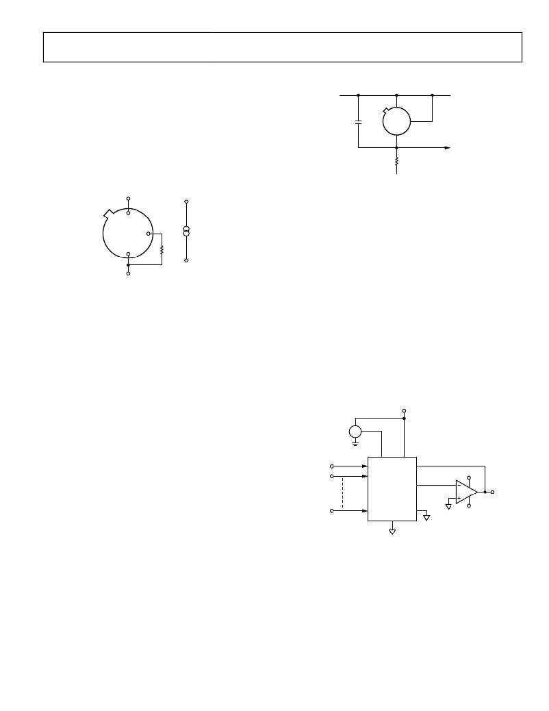
�10� V� REFERENCE� WITH� MULTIPLYING� CMOS� DACs�
�OR� ADCs�
�i� ~� =� ___� +� 0.75mA�
�AD581�
�V� OUT�
�GND�
�10V� =�
�R�
�LOAD�
�10V�
�R�
�The� AD581� is� ideal� for� application� with� the� entire� AD7533�
�series� of� 10-� and� 12-bit� multiplying� CMOS� DACs,� especially� for�
�low� power� applications.� It� is� equally� suitable� for� the� AD7574�
�8-bit� ADC.� In� the� standard� hook-up,� as� shown� in� Figure� 15,� the�
�BOTTOM� VIEW� OF�
�10V� PRECISION�
�REFERENCE� CIRCUIT�
�IN� TO-5� CASE�
�Figure� 12.� A� Two-Component� Precision� Current� Limiter�
�NEGATIVE� 10� V� REFERENCE�
�The� AD581� can� also� be� used� in� a� 2-pin� Zener� mode� to� provide� a�
�precision� ?10.00� V� reference.� As� shown� in� Figure� 13,� the� +V� S� and�
�V� OUT� pins� are� connected� together� to� the� high� supply� (in� this�
�case,� ground).� The� ground� pin� is� connected� through� a� resistor�
�to� the� negative� supply.� Thus,� the� output� is� taken� from� the�
�ground� pin� instead� of� V� OUT� .� With� 1� mA� flowing� through� the�
�AD581� in� this� mode,� a� typical� unit� shows� a� 2� mV� increase� in�
�output� level� over� that� produced� in� the� 3-pin� mode.� Note� also�
�that� the� effective� output� impedance� in� this� connection� increases�
�+10� V� reference� is� inverted� by� the� amplifier/DAC� configuration�
�to� produce� a� 0� V� to� ?10� V� range.� If� an� OP1177� amplifier� is� used,�
�total� quiescent� supply� current� is� typically� 2� mA.� If� a� 0� V� to� +10� V�
�full-scale� range� is� desired,� the� AD581� can� be� connected� to� the�
��(the� ?10� V� REF� output� is� connected� directly� to� the� V� REF� IN� of� the�
�CMOS� DAC).� The� AD581� is� normally� used� in� the� ?10� V� mode�
�with� the� AD7574� to� give� a� 0� V� to� +10� V� ADC� range.� This� is�
�shown� in� Figure� 15.� Bipolar� output� applications� and� other�
�operating� details� can� be� found� in� the� data� sheets� for� the� CMOS�
�products.�
�+15V�
�+10V�
�AD581�
�from� 0.2� Ω� typical� to� 2� Ω.� It� is� essential� to� arrange� the� output�
�load� and� the� supply� resistor,� R� S� ,� so� that� the� net� current� through�
�the� AD581� is� always� between� 1� mA� and� 5� mA.� For� operation� to�
�+125°C,� the� net� current� should� be� between� 2� mA� and� 5� mA.� The�
�DIGITAL�
�INPUT�
�V� REF� IN�
�BIT� 1� (MSB)�
�4�
�5�
�15�
�14�
�16�
�1�
�R� FEEDBACK�
�I� OUT1�
�+15V�
�temperature� characteristics� and� long-term� stability� of� the� device�
�V� OUT�
�are� essentially� the� same� as� that� of� a� unit� used� in� the� standard�
�I� OUT2�
�0V� TO� –10V�
�3-pin� mode.�
�BIT� 10� (LSB)�
�13�
�3�
�2�
�–15V�
�The� AD581� can� also� be� used� in� a� 2-pin� mode� to� develop� a�
�positive� reference.� +V� S� and� V� OUT� are� tied� together� and� to� the�
�positive� supply� through� an� appropriate� supply� resistor.� The�
�performance� characteristics� are� similar� to� those� of� the� negative�
�2-pin� connection.� The� only� advantage� of� this� connection� over�
�the� standard� 3-pin� connection� is� that� a� lower� primary� supply�
�can� be� used,� as� low� as� 10.5� V.� This� type� of� operation� requires� con-�
�siderable� attention� to� load� and� primary� supply� regulation� to�
�maintain� the� AD581� within� its� regulating� range� of� 1� mA� to� 5� mA�
�(2� mA� to� 5� mA� for� operation� beyond� +85°C).�
�GND�
�Figure� 14.� Low� Power� 10-Bit� CMOS� DAC� Application�
�PRECISION� 12-BIT� DAC� REFERENCE�
�AD565A,� like� most� DACs,� is� designed� to� operate� with� a� +10� V�
�reference� element.� In� the� AD565A,� this� 10� V� reference� voltage� is�
�converted� into� a� reference� current� of� approximately� 0.5� mA� via�
�the� internal� 19.95� k� resistor� (in� series� with� the� external� 100� �
�trimmer).� The� gain� temperature� coefficient� of� the� AD565A� is�
�primarily� governed� by� the� temperature� tracking� of� the� 19.95� k�
�resistor� and� the� 5� k� to10� k� span� resistors;� gain� TC� is� guaran-�
�teed� to� 3� ppm/°C.� Thus,� using� the� AD581L� (at� 5� ppm/°C)� as� the�
�Rev.� C� |� Page� 9� of� 12�
�相关PDF资料 |
PDF描述 |
|---|---|
| VI-JNP-EW-B1 | CONVERTER MOD DC/DC 13.8V 100W |
| GBM10DCSH-S288 | CONN EDGECARD 20POS .156 EXTEND |
| VI-JNP-CX-F4 | CONVERTER MOD DC/DC 13.8V 75W |
| GBM24DCMS | CONN EDGECARD 48POS .156 WW |
| VI-JNP-CX-F3 | CONVERTER MOD DC/DC 13.8V 75W |
相关代理商/技术参数 |
参数描述 |
|---|---|
| AD581JH/+ | 制造商:Rochester Electronics LLC 功能描述:- Bulk |
| AD581JHZ | 制造商:Analog Devices 功能描述: |
| AD581K | 制造商:AD 制造商全称:Analog Devices 功能描述:High Precision 10 V IC Reference |
| AD581KCSA | 制造商:未知厂家 制造商全称:未知厂家 功能描述:Voltage Reference |
| AD581KH | 功能描述:IC VREF SERIES PREC 10V TO-5-3 RoHS:是 类别:集成电路 (IC) >> PMIC - 电压基准 系列:- 标准包装:3,000 系列:- 基准类型:旁路,精度 输出电压:3V 容差:±0.5% 温度系数:100ppm/°C 输入电压:- 通道数:1 电流 - 阴极:82µA 电流 - 静态:- 电流 - 输出:15mA 工作温度:-40°C ~ 85°C 安装类型:表面贴装 封装/外壳:6-TSSOP(5 引线),SC-88A,SOT-353 供应商设备封装:SC-70-5 包装:带卷 (TR) 其它名称:296-20888-2 |
发布紧急采购,3分钟左右您将得到回复。