- 您现在的位置:买卖IC网 > PDF目录20681 > AD584TH (Analog Devices Inc)IC VREF SERIES PREC ADJ TO-99-8 PDF资料下载
参数资料
| 型号: | AD584TH |
| 厂商: | Analog Devices Inc |
| 文件页数: | 6/12页 |
| 文件大小: | 0K |
| 描述: | IC VREF SERIES PREC ADJ TO-99-8 |
| 标准包装: | 1 |
| 基准类型: | 串联,可调节,精度 |
| 输出电压: | 2.5V,5V,7.5V,10V |
| 容差: | ±10% |
| 温度系数: | 15ppm/°C |
| 输入电压: | 4.5 V ~ 30 V |
| 通道数: | 1 |
| 电流 - 静态: | 1mA |
| 电流 - 输出: | 10mA |
| 工作温度: | -55°C ~ 125°C |
| 安装类型: | 通孔 |
| 封装/外壳: | TO-99-8 金属罐 |
| 供应商设备封装: | TO-99-8 |
| 包装: | 散装 |
| 产品目录页面: | 795 (CN2011-ZH PDF) |
�� ��
��
��AD584�
�THEORY� OF� OPERATION�
�APPLYING� THE� AD584�
�With� power� applied� to� Pin� 8� and� Pin� 4� and� all� other� pins� open,�
�the� AD584� produces� a� buffered� nominal� 10.0� V� output� between�
�Pin� 1� and� Pin� 4� (see� Figure� 3).� The� stabilized� output� voltage� can�
�be� reduced� to� 7.5� V,� 5.0� V,� or� 2.5� V� by� connecting� the� programming�
��Data� Sheet�
�approximately� 20� V,� even� for� the� large� values� of� R1.� Do� not�
�omit� R2;� choose� its� value� to� limit� the� output� to� a� value� that� can�
�be� tolerated� by� the� load� circuits.� If� R2� is� zero,� adjusting� R1� to� its�
�lower� limit� results� in� a� loss� of� control� over� the� output� voltage.�
�When� precision� voltages� are� set� at� levels� other� than� the� standard�
�outputs,� account� for� the� 20%� absolute� tolerance� in� the� internal�
�resistor� ladder.�
�Table� 4.�
�Output�
�Voltage� (V)�
�7.5�
�5.0�
�2.5�
�Pin� Programming�
�Join� the� 2.5� V� (Pin� 3)� and� 5.0� V� (Pin� 2)� pins.�
�Connect� the� 5.0� V� pin� (Pin� 2)� to� the� output� pin� (Pin� 1).�
�Connect the 2.5 V pin (Pin 3) to the output pin (Pin 1).�
�Alternatively,� the� output� voltage� can� be� raised� by� loading� the�
�2.5� V� tap� with� R3� alone.� The� output� voltage� can� be� lowered� by�
�connecting� R4� alone.� Either� of� these� resistors� can� be� a� fixed�
�resistor� selected� by� test� or� an� adjustable� resistor.� In� all� cases,� the�
�resistors� should� have� a� low� temperature� coefficient� to� match� the�
�AD584� internal� resistors,� which� have� a� negative� temperature�
�The� options� shown� in� Table� 4� are� available� without� the� use� of� any�
�additional� components.� Multiple� outputs� using� only� one� AD584�
�can� be� provided� by� buffering� each� voltage� programming� pin�
�with� a� unity-gain,� noninverting� op� amp.�
�coefficient� less� than� 60� ppm/°C.� If� both� R3� and� R4� are� used,�
�these� resistors� should� have� matching� temperature� coefficients.�
�When� only� small� adjustments� or� trims� are� required,� the� circuit�
�in� Figure� 4� offers� better� resolution� over� a� limited� trim� range.� The�
�AD584�
�1.215V�
�8�
�*�
�V� SUPPLY�
�10V�
�24k?�
�5V�
�12k?�
�1�
�2�
�V� OUT�
�R4�
�circuit� can� be� programmed� to� 5.0� V,� 7.5� V,� or� 10� V,� and� it� can� be�
�adjusted� by� means� of� R1� over� a� range� of� about� ±200� mV.� To� trim�
�the� 2.5� V� output� option,� R2� (see� Figure� 4)� can� be� reconnected� to�
�the� band� gap� reference� (Pin� 6).� In� this� configuration,� limit� the�
�adjustment� to� ±100� mV� to� avoid� affecting� the� performance� of�
��V+�
�2.5V�
�R1�
�V� BG�
�6k?�
�3�
�R3�
�8�
�1�
�10.0V�
�V� OUT�
�COMMON�
�4�
�6k?�
�6�
�R2�
�AD584�
�2�
�3�
�6�
�5.0V�
�2.5V�
�V� BG�
�R2�
�300k?�
�R1�
�10k?�
�*� THE� 2.5V� TAP� IS� USED� INTERNALLY� AS� A� BIAS� POINT�
�AND� SHOULD� NOT� BE� CHANGED� BY� MORE� THAN� 100mV�
�4�
�Q11�
�IN� ANY� TRIM� CONFIGURATION.�
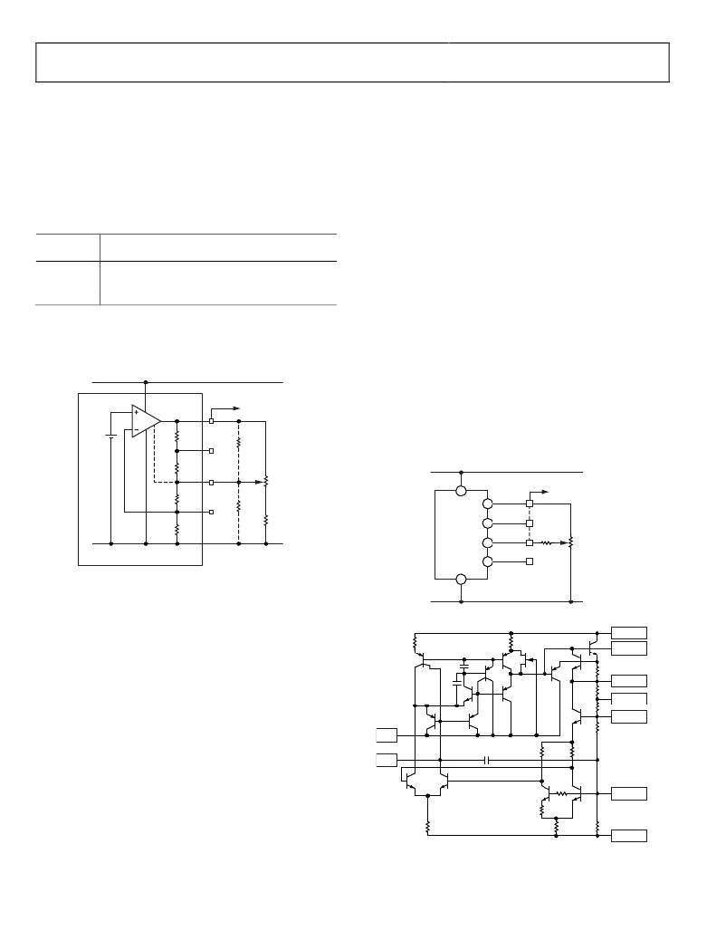
�Figure� 3.� Variable� Output� Options�
�The� AD584� can� also� be� programmed� over� a� wide� range� of� output�
�voltages,� including� voltages� greater� than� 10� V,� by� the� addition�
�of� one� or� more� external� resistors.� Figure� 3� illustrates� the� general�
�adjustment� procedure,� with� approximate� values� given� for� the�
�internal� resistors� of� the� AD584� .� The� AD584� may� be� modeled�
�as� an� op� amp� with� a� noninverting� feedback� connection,� driven�
�by� a� high� stability� 1.215� V� band� gap� reference� (see� Figure� 5� for�
�schematic).�
�SUB�
�R40�
�Q10�
�Q16�
�COMMON�
�Figure� 4.� Output� Trimming�
�R41�
�Q20�
�Q8�
�C52�
�Q12� Q15�
�C51� Q6� Q14�
�Q5�
�Q13�
�R42�
�R34�
�R37�
�R35�
�Q7�
�V+�
�STROBE�
�OUT� 10V�
�5V� TAP�
�2.5V� TAP�
�When� the� feedback� ratio� is� adjusted� with� external� resistors,� the�
�output� amplifier� can� be� made� to� multiply� the� reference� voltage�
�CAP�
�C50�
�R33�
�R32�
�by� almost� any� convenient� amount,� making� popular� outputs� of�
�10.24� V,� 5.12� V,� 2.56� V,� or� 6.3� V� easy� to� obtain.� The� most� general�
�adjustment� (which� gives� the� greatest� range� and� poorest� resolution)�
�uses� R1� and� R2� alone� (see� Figure� 3).� As� R1� is� adjusted� to� its� upper�
�limit,� the� 2.5V� pin� (Pin� 3)� is� connected� to� the� output,� which�
�Q3�
�Q4�
�R39�
�R� 38�
�Q2�
�R30�
�R31�
�Q1�
�R36�
�V� BG�
�V–�
�reduces� to� 2.5� V.� As� R1� is� adjusted� to� its� lower� limit,� the� output�
�voltage� rises� to� a� value� limited� by� R2.� For� example,� if� R2� is�
�approximately� 6� kΩ,� the� upper� limit� of� the� output� range� is�
�Rev.� C� |� Page� 6� of� 12�
�Figure� 5.� Schematic� Diagram�
�相关PDF资料 |
PDF描述 |
|---|---|
| ESC60DRYI-S13 | CONN EDGECARD 120POS .100 EXTEND |
| ECM08DCAT-S189 | CONN EDGECARD 16POS R/A .156 SLD |
| 572D336X96R3A2T | CAP TANT 33UF 6.3V 10% 1206 |
| T95S335M016HSAL | CAP TANT 3.3UF 16V 20% 1507 |
| RW2-4812D/H2/B | CONV DC/DC 2W 36-72VIN +/-12VOUT |
相关代理商/技术参数 |
参数描述 |
|---|---|
| AD584TH/883 | 制造商:未知厂家 制造商全称:未知厂家 功能描述:Voltage Reference |
| AD584TH/883B | 制造商:Analog Devices 功能描述:V-Ref Programmable 2.5V/5V/7.5V/10V 10mA 8-Pin TO-99 制造商:Analog Devices 功能描述:V-REF PROGRAMMABLE 2.5V/5V/7.5V/10V 10MA 8PIN TO-99 - Rail/Tube 制造商:Analog Devices 功能描述:IC - PROGRAMMABLE V REF. 制造商:Analog Devices 功能描述:IC VOLT REF PROG 制造商:Analog Devices Inc. 功能描述:Voltage & Current References IC PROG V REF |
| AD584TH/HR | 制造商:未知厂家 制造商全称:未知厂家 功能描述:Voltage Reference |
| AD584TQ | 制造商:未知厂家 制造商全称:未知厂家 功能描述:Voltage Reference |
| AD584TQ/883 | 制造商:未知厂家 制造商全称:未知厂家 功能描述:Voltage Reference |
发布紧急采购,3分钟左右您将得到回复。