- 您现在的位置:买卖IC网 > PDF目录10979 > AD5933YRSZ (Analog Devices Inc)IC NTWK ANALYZER 12B 1MSP 16SSOP PDF资料下载
参数资料
| 型号: | AD5933YRSZ |
| 厂商: | Analog Devices Inc |
| 文件页数: | 7/40页 |
| 文件大小: | 0K |
| 描述: | IC NTWK ANALYZER 12B 1MSP 16SSOP |
| 产品培训模块: | AD5933 Impedance to Digital Converter Direct Digital Synthesis Tutorial Series (1 of 7): Introduction Direct Digital Synthesizer Tutorial Series (7 of 7): DDS in Action Direct Digital Synthesis Tutorial Series (3 of 7): Angle to Amplitude Converter Direct Digital Synthesis Tutorial Series (6 of 7): SINC Envelope Correction Direct Digital Synthesis Tutorial Series (4 of 7): Digital-to-Analog Converter Direct Digital Synthesis Tutorial Series (2 of 7): The Accumulator |
| 标准包装: | 1 |
| 分辨率(位): | 12 b |
| 主 fclk: | 16.776MHz |
| 电源电压: | 2.7 V ~ 5.5 V |
| 工作温度: | -40°C ~ 125°C |
| 安装类型: | 表面贴装 |
| 封装/外壳: | 16-SSOP(0.209",5.30mm 宽) |
| 供应商设备封装: | 16-SSOP |
| 包装: | 管件 |
| 产品目录页面: | 797 (CN2011-ZH PDF) |
| 配用: | EVAL-AD5933EBZ-ND - BOARD EVALUATION FOR AD5933 |
| 其它名称: | AD5933BRSZ-ND Q2204656A |
第1页第2页第3页第4页第5页第6页当前第7页第8页第9页第10页第11页第12页第13页第14页第15页第16页第17页第18页第19页第20页第21页第22页第23页第24页第25页第26页第27页第28页第29页第30页第31页第32页第33页第34页第35页第36页第37页第38页第39页第40页
Data Sheet
AD5933
Rev. E | Page 15 of 40
FREQUENCY SWEEP COMMAND SEQUENCE
The following sequence must be followed to implement a
frequency sweep:
1. Enter standby mode. Prior to issuing a start frequency sweep
command, the device must be placed in a standby mode by
issuing an enter standby mode command to the control
register (Register Address 0x80 and Register Address 0x81).
In this mode, the VOUT and VIN pins are connected
internally to ground so there is no dc bias across the external
impedance or between the impedance and ground.
2. Enter initialize mode. In general, high Q complex circuits
require a long time to reach steady state. To facilitate the
measurement of such impedances, this mode allows the user
full control of the settling time requirement before entering
start frequency sweep mode where the impedance
measurement takes place.
An initialize with a start frequency command to the control
register enters initialize mode. In this mode the impedance
is excited with the programmed start frequency, but no meas-
urement takes place. The user times out the required settling
time before issuing a start frequency sweep command to the
control register to enter the start frequency sweep mode.
3. Enter start frequency sweep mode. The user enters this mode
by issuing a start frequency sweep command to the control
register. In this mode, the ADC starts measuring after the
programmed number of settling time cycles has elapsed. The
user can program an integer number of output frequency
cycles (settling time cycles) to Register Address 0x8A and
Register Address 0x8B before beginning the measurement
at each frequency point (see Figure 28).
The DDS output signal is passed through a programmable gain
stage to generate the four ranges of peak-to-peak output excitation
signals listed in Table 5. The peak-to-peak output excitation volt-
age is selected by setting Bit D10 and Bit D9 in the control register
Address 0X81) section) and is made available at the VOUT pin.
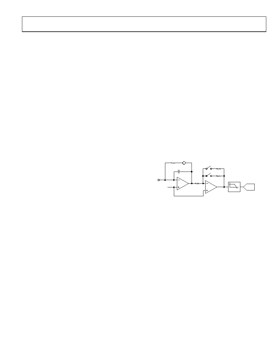
RECEIVE STAGE
The receive stage comprises a current-to-voltage amplifier,
followed by a programmable gain amplifier (PGA), antialiasing
filter, and ADC. The receive stage schematic is shown in
Figure 20. The unknown impedance is connected between the
VOUT and VIN pins. The first stage current-to-voltage amplifier
configuration means that a voltage present at the VIN pin is a
virtual ground with a dc value set at VDD/2. The signal current
that is developed across the unknown impedance flows into the
VIN pin and develops a voltage signal at the output of the current-
to-voltage converter. The gain of the current-to voltage amplifier
is determined by a user-selectable feedback resistor connected
between Pin 4 (RFB) and Pin 5 (VIN). It is important for the user
to choose a feedback resistance value that, in conjunction with the
selected gain of the PGA stage, maintains the signal within the
linear range of the ADC (0 V to VDD).
The PGA allows the user to gain the output of the current-to-
voltage amplifier by a factor of 5 or 1, depending upon the status
of Bit D8 in the control register (see the Register Map section,
Register Address 0x80). The signal is then low-pass filtered and
presented to the input of the 12-bit, 1 MSPS ADC.
5 × R
R
C
VIN
VDD/2
RFB
ADC
LPF
05324-
020
Figure 20. Receive Stage
The digital data from the ADC is passed directly to the DSP core
of the AD5933, which performs a DFT on the sampled data.
DFT OPERATION
A DFT is calculated for each frequency point in the sweep. The
AD5933 DFT algorithm is represented by
∑
=
=
1023
0
)))
sin(
)
)(cos(
(
)
(
n
j
n
x
f
X
where:
X(f) is the power in the signal at the Frequency Point f.
x(n) is the ADC output.
cos(n) and sin(n) are the sampled test vectors provided by the
DDS core at the Frequency Point f.
The multiplication is accumulated over 1024 samples for each
frequency point. The result is stored in two, 16-bit registers
representing the real and imaginary components of the result.
The data is stored in twos complement format.
相关PDF资料 |
PDF描述 |
|---|---|
| MC908JL3EMPE | IC MCU 4K FLASH W/OSC 28-PDIP |
| MC908AP8CFAE | IC MCU 8K FLASH 8MHZ 48-LQFP |
| AD9851BRSZ | IC SYNTHESIZER DDS/DAC 28-SSOP |
| S9S08DZ96F2MLF | MCU 96K FLASH MASK AUTO 48-LQFP |
| AD9850BRSZ | IC DDS SYNTHESIZER CMOS 28-SSOP |
相关代理商/技术参数 |
参数描述 |
|---|---|
| AD5933YRSZ | 制造商:Analog Devices 功能描述:IC IMPEDANCE CONV 1MSPS 12BIT 16SSOP |
| AD5933YRSZ-REEL7 | 功能描述:NETWORK ANALYZER 12B 1MSP 16SSOP RoHS:是 类别:集成电路 (IC) >> 接口 - 直接数字合成 (DDS) 系列:- 产品变化通告:Product Discontinuance 27/Oct/2011 标准包装:2,500 系列:- 分辨率(位):10 b 主 fclk:25MHz 调节字宽(位):32 b 电源电压:2.97 V ~ 5.5 V 工作温度:-40°C ~ 85°C 安装类型:表面贴装 封装/外壳:16-TSSOP(0.173",4.40mm 宽) 供应商设备封装:16-TSSOP 包装:带卷 (TR) |
| AD5934 | 制造商:Analog Devices 功能描述:IMPEDANCE TO DIGITAL CONVERTERS - Bulk |
| AD5934YRSZ | 功能描述:IC NTWK ANALYZER 12B 1MSP 16SSOP RoHS:是 类别:集成电路 (IC) >> 接口 - 直接数字合成 (DDS) 系列:- 产品变化通告:Product Discontinuance 27/Oct/2011 标准包装:2,500 系列:- 分辨率(位):10 b 主 fclk:25MHz 调节字宽(位):32 b 电源电压:2.97 V ~ 5.5 V 工作温度:-40°C ~ 85°C 安装类型:表面贴装 封装/外壳:16-TSSOP(0.173",4.40mm 宽) 供应商设备封装:16-TSSOP 包装:带卷 (TR) |
| AD5934YRSZ-REEL7 | 功能描述:IC CONV 12BIT 250KSPS 16SSOP RoHS:是 类别:集成电路 (IC) >> 接口 - 直接数字合成 (DDS) 系列:- 产品变化通告:Product Discontinuance 27/Oct/2011 标准包装:2,500 系列:- 分辨率(位):10 b 主 fclk:25MHz 调节字宽(位):32 b 电源电压:2.97 V ~ 5.5 V 工作温度:-40°C ~ 85°C 安装类型:表面贴装 封装/外壳:16-TSSOP(0.173",4.40mm 宽) 供应商设备封装:16-TSSOP 包装:带卷 (TR) |
发布紧急采购,3分钟左右您将得到回复。