- 您现在的位置:买卖IC网 > Datasheet目录38 > AD595CD (Analog Devices Inc)IC THERMOCOUPLE INSTR AMP 14CDIP Datasheet资料下载
参数资料
| 型号: | AD595CD |
| 厂商: | Analog Devices Inc |
| 文件页数: | 5/8页 |
| 文件大小: | 136K |
| 描述: | IC THERMOCOUPLE INSTR AMP 14CDIP |
| 产品变化通告: | Product Discontinuance 27/Oct/2011 |
| 标准包装: | 1 |
| 功能: | 热电偶放大器 |
| 传感器类型: | 外部 |
| 精确度: | ±1°C(最小值) |
| 拓扑: | 冰点补偿,过载检测 |
| 输出类型: | 电压 |
| 输出警报: | 是 |
| 输出风扇: | 无 |
| 电源电压: | 5 V ~ ±15 V |
| 工作温度: | -55°C ~ 125°C |
| 安装类型: | 通孔 |
| 封装/外壳: | 14-CDIP(0.300",7.62mm) |
| 供应商设备封装: | 14-CDIP |
| 包装: | 管件 |
AD594/AD595
REV. C
5
The AD594/AD595 also includes an input open circuit detector
that switches on an alarm transistor. This transistor is actually a
current-limited output buffer, but can be used up to the limit as
a switch transistor for either pull-up or pull-down operation of
external alarms.
The ice point compensation network has voltages available with
positive and negative temperature coefficients. These voltages
may be used with external resistors to modify the ice point com-
pensation and recalibrate the AD594/AD595 as described in the
next column.
The feedback resistor is separately pinned out so that its value
can be padded with a series resistor, or replaced with an external
resistor between Pins 5 and 9. External availability of the feedback
resistor allows gain to be adjusted, and also permits the AD594/
AD595 to operate in a switching mode for setpoint operation.
CAUTIONS:
The temperature compensation terminals (+C and C) at Pins 2
and 6 are provided to supply small calibration currents only. The
AD594/AD595 may be permanently damaged if they are
grounded or connected to a low impedance.
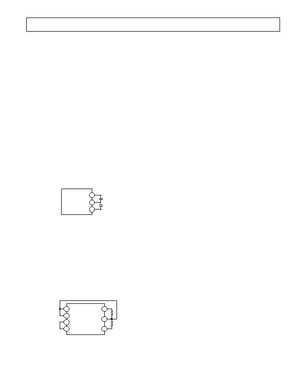
The AD594/AD595 is internally frequency compensated for feed-
back ratios (corresponding to normal signal gain) of 75 or more.
If a lower gain is desired, additional frequency compensation
should be added in the form of a 300 pF capacitor from Pin 10
to the output at Pin 9. As shown in Figure 5 an additional 0.01 礔
capacitor between Pins 10 and 11 is recommended.
AD594/
AD595
VO
COMP
+V
9
10
11
300pF
0.01F
Figure 5. Low Gain Frequency Compensation
RECALIBRATION PRINCIPLES AND LIMITATIONS
The ice point compensation network of the AD594/AD595
produces a differential signal which is zero at 0癈 and corre-
sponds to the output of an ice referenced thermocouple at the
temperature of the chip. The positive TC output of the circuit is
proportional to Kelvin temperature and appears as a voltage at
+T. It is possible to decrease this signal by loading it with a
resistor from +T to COM, or increase it with a pull-up resistor
from +T to the larger positive TC voltage at +C. Note that
adjustments to +T should be made by measuring the voltage which
tracks it at T. To avoid destabilizing the feedback amplifier the
measuring instrument should be isolated by a few thousand
ohms in series with the lead connected to T.
AD594/
AD595
+IN
IN
+T
COM
T
FB
VO
9
1
14
8
3
4
5
Figure 6. Decreased Sensitivity Adjustment
Changing the positive TC half of the differential output of the
compensation scheme shifts the zero point away from 0癈. The
zero can be restored by adjusting the current flow into the nega-
tive input of the feedback amplifier, the T pin. A current into
this terminal can be produced with a resistor between C and
T to balance an increase in +T, or a resistor from T to COM
to offset a decrease in +T.
If the compensation is adjusted substantially to accommodate a
different thermocouple type, its effect on the final output volt-
age will increase or decrease in proportion. To restore the
nominal output to 10 mV/癈 the gain may be adjusted to match
the new compensation and thermocouple input characteristics.
When reducing the compensation the resistance between T
and COM automatically increases the gain to within 0.5% of the
correct value. If a smaller gain is required, however, the nominal
47 k& internal feedback resistor can be paralleled or replaced
with an external resistor.
Fine calibration adjustments will require temperature response
measurements of individual devices to assure accuracy. Major
reconfigurations for other thermocouple types can be achieved
without seriously compromising initial calibration accuracy, so
long as the procedure is done at a fixed temperature using the
factory calibration as a reference. It should be noted that inter-
mediate recalibration conditions may require the use of a
negative supply.
EXAMPLE: TYPE E RECALIBRATIONAD594/AD595
Both the AD594 and AD595 can be configured to condition the
output of a type E (chromel-constantan) thermocouple. Tem-
perature characteristics of type E thermocouples differ less from
type J, than from type K, therefore the AD594 is preferred for
recalibration.
While maintaining the device at a constant temperature follow
the recalibration steps given here. First, measure the device
temperature by tying both inputs to common (or a selected
common-mode potential) and connecting FB to VO. The AD594
is now in the stand alone Celsius thermometer mode. For this
example assume the ambient is 24癈 and the initial output VO
is 240 mV. Check the output at VO to verify that it corresponds
to the temperature of the device.
Next, measure the voltage T at Pin 5 with a high impedance
DVM (capacitance should be isolated by a few thousand ohms
of resistance at the measured terminals). At 24癈 the T voltage
will be about 8.3 mV. To adjust the compensation of an AD594
to a type E thermocouple a resistor, R1, should be connected
between +T and +C, Pins 2 and 3, to raise the voltage at T by
the ratio of thermocouple sensitivities. The ratio for converting a
type J device to a type E characteristic is:
r (AD594) =(60.9 ?/SPAN>V/?/SPAN>C)/(51.7 ?/SPAN>V/?/SPAN>C)= 1.18
Thus, multiply the initial voltage measured at T by r and ex-
perimentally determine the R1 value required to raise T to that
level. For the example the new T voltage should be about 9.8 mV.
The resistance value should be approximately 1.8 k&.
The zero differential point must now be shifted back to 0癈.
This is accomplished by multiplying the original output voltage
VO by r and adjusting the measured output voltage to this value
by experimentally adding a resistor, R2, between C and T,
Pins 5 and 6. The target output value in this case should be
about 283 mV. The resistance value of R2 should be approxi-
mately 240 k&.
Finally, the gain must be recalibrated such that the output VO
indicates the devices temperature once again. Do this by adding
a third resistor, R3, between FB and T, Pins 8 and 5. VO should
now be back to the initial 240 mV reading. The resistance value
相关PDF资料 |
PDF描述 |
|---|---|
| AD597AHZ | IC THERMOCOUPLE COND TO-100-10 |
| AD7314ARMZ-REEL7 | IC SENSOR TEMP 10BIT DGTL 8-MSOP |
| AD7814ARTZ-REEL | IC TEMP SNSR 10BIT DGTL SOT23-6 |
| AD7818ARZ | IC ADC 10BIT W/TEMP SENSOR 8SOIC |
| AD8210WYRZ-R7 | IC CURRENT MONITOR 0.5% 8SOIC |
相关代理商/技术参数 |
参数描述 |
|---|---|
| AD595CDZ | 功能描述:IC THERMOCOUPLE INSTR AMP 14CDIP RoHS:是 类别:集成电路 (IC) >> PMIC - 热管理 系列:- 标准包装:3,000 系列:- 功能:温度开关 传感器类型:内部 感应温度:85°C 分界点 精确度:±6°C(最小值) 拓扑:ADC(三角积分型),比较器,寄存器库 输出类型:开路漏极 输出警报:是 输出风扇:是 电源电压:2.7 V ~ 5.5 V 工作温度:-55°C ~ 125°C 安装类型:表面贴装 封装/外壳:SC-74A,SOT-753 供应商设备封装:SOT-23-5 包装:带卷 (TR) 其它名称:ADT6501SRJZP085RL7-ND |
| AD595CDZ | 制造商:Analog Devices 功能描述:IC INSTRUMENTATION AMPLIFIER TO116-14 |
| AD595CQ | 功能描述:IC THERMOCOUPLE A W/COMP 14CDIP RoHS:否 类别:集成电路 (IC) >> PMIC - 热管理 系列:- 标准包装:3,000 系列:- 功能:温度开关 传感器类型:内部 感应温度:85°C 分界点 精确度:±6°C(最小值) 拓扑:ADC(三角积分型),比较器,寄存器库 输出类型:开路漏极 输出警报:是 输出风扇:是 电源电压:2.7 V ~ 5.5 V 工作温度:-55°C ~ 125°C 安装类型:表面贴装 封装/外壳:SC-74A,SOT-753 供应商设备封装:SOT-23-5 包装:带卷 (TR) 其它名称:ADT6501SRJZP085RL7-ND |
| AD596 | 制造商:AD 制造商全称:Analog Devices 功能描述:Thermocouple Conditioner and Setpoint Controller |
发布紧急采购,3分钟左右您将得到回复。