参数资料
| 型号: | AD600ARZ-R7 |
| 厂商: | Analog Devices Inc |
| 文件页数: | 17/33页 |
| 文件大小: | 0K |
| 描述: | IC AMP VGA DUAL LN 50MA 16SOIC |
| 标准包装: | 400 |
| 系列: | X-AMP® |
| 放大器类型: | 可变增益 |
| 电路数: | 2 |
| 转换速率: | 275 V/µs |
| -3db带宽: | 35MHz |
| 电流 - 输入偏压: | 350nA |
| 电流 - 电源: | 11mA |
| 电流 - 输出 / 通道: | 50mA |
| 电压 - 电源,单路/双路(±): | ±4.75 V ~ 5.25 V |
| 工作温度: | -40°C ~ 85°C |
| 安装类型: | 表面贴装 |
| 封装/外壳: | 16-SOIC(0.295",7.50mm 宽) |
| 供应商设备封装: | 16-SOIC W |
| 包装: | 带卷 (TR) |
第1页第2页第3页第4页第5页第6页第7页第8页第9页第10页第11页第12页第13页第14页第15页第16页当前第17页第18页第19页第20页第21页第22页第23页第24页第25页第26页第27页第28页第29页第30页第31页第32页第33页
AD600/AD602
Rev. F | Page 23 of 32
2.0
–2.0
0.5
1.0
1.5
–1.5
–1.0
–0.5
GA
IN
E
R
OR
(
d
B
)
–0.1
0.1
0
1
10
1
100m
10m
1m
100
INPUT SIGNAL (V rms)
00
53
8-
04
7
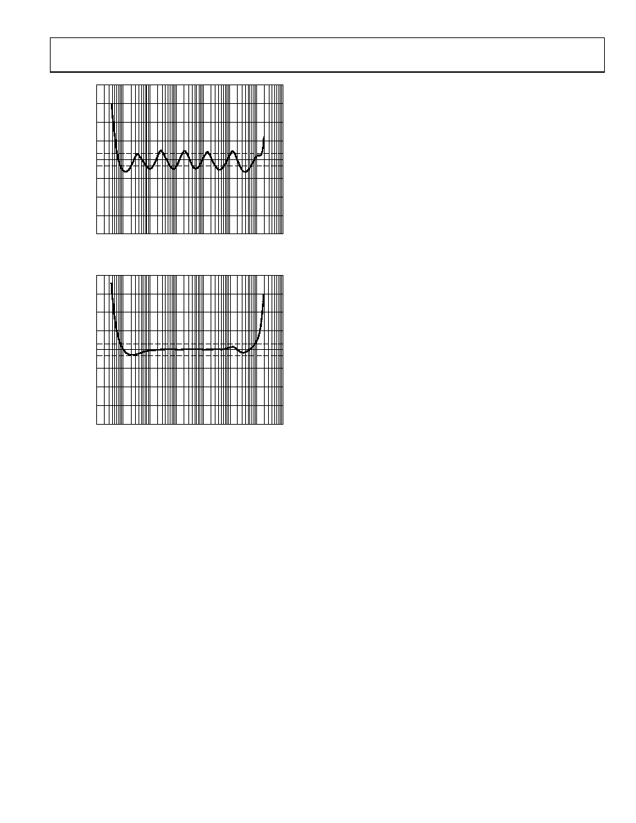
Figure 49. Gain Error for Figure 41 Without the 2 dB Offset Modification
2.0
–2.0
0.5
1.0
1.5
–1.5
–1.0
–0.5
GA
IN
E
R
OR
(
d
B
)
–0.1
0.1
0
1
10
1
100m
10m
1m
100
INPUT SIGNAL (V rms)
00
53
8-
0
48
Figure 50. Adding the 2 dB Offsets Improves the Linearization
The maximum gain of this circuit is 120 dB. If no filtering were
used, the noise spectral density of the AD600 (1.4 nV/√Hz)
would amount to an input noise of 8.28 μV rms in the full
bandwidth (35 MHz). At a gain of one million, the output noise
would dominate. Consequently, some reduction of bandwidth is
mandatory and, in the circuit of Figure 47, it is due mostly to a
single-pole, low-pass filter R5/C3 that provides a 3 dB
frequency of 458 kHz, which reduces the worst-case output
noise (at VAGC) to about 100 mV rms at a gain of 100 dB. Of
course, the bandwidth (and therefore the output noise) could be
further reduced, for example, in audio applications, merely by
increasing C3. The value chosen for this application is optimal
in minimizing the error in the VLOG output for small input signals.
The AD600 is dc-coupled, but even miniscule offset voltages at
the input would overload the output at high gains; thus, high-
pass filtering is also needed. To provide operation at low
frequencies, two simple 0s at about 12 Hz are provided by
R1/C1 and R4/C2; the U3A and U3B (AD713) op amp sections
are used to provide impedance buffering because the input
resistance of the AD600 is only 100 Ω. A further 0 at 12 Hz is
provided by C4 and the 6.7 kΩ input resistance of the AD636
rms converter.
The rms value of VLOG is generated at Pin 8 of the AD636; the
averaging time for this process is determined by C5, and the
value shown results in less than 1% rms error at 20 Hz. The
slowly varying V rms is compared with a fixed reference of
316 mV, derived from the positive supply by R10/R11. Any
difference between these two voltages is integrated in C6, in
conjunction with the U3C op amp, the output of which is VLOG.
A fraction of this voltage, determined by R12 and R13, is
returned to the gain control inputs of all AD600 sections.
An increase in VLOG lowers the gain because this voltage is
connected to the inverting polarity control inputs.
In this case, the gains of all three VCA sections are varied
simultaneously, so the scaling is not 32 dB/V but 96 dB/V or
10.42 mV/dB. The fraction of VLOG required to set its scaling to
50 mV/dB is therefore 10.42/50 or 0.208. The resulting full-
scale range of VLOG is nominally ±2.5 V. This scaling allows the
circuit to operate from ±5 V supplies.
Optionally, the scaling can be altered to 100 mV/dB, which
would be more easily interpreted when VLOG is displayed on a
DVM by increasing R12 to 25.5 kΩ. The full-scale output of
±5 V then requires the use of supply voltages of at least ±7.5 V.
A simple attenuator of 16.6 ± 1.25 dB is formed by R2/R3
and the 100 Ω input resistance of the AD600. This allows the
reference level of the decibel output to be precisely set to 0 for
an input of 3.16 mV rms and thus center the 100 dB range
between 10 μV and 1 V. In many applications, R2/R3 can be
replaced by a fixed resistor of 590 Ω. For example, in AGC
applications, neither the slope nor the intercept of the
logarithmic output is important.
A few additional components (R14 to R16 and Q1) improve the
accuracy of VLOG at the top end of the signal range (that is, for
small gains). The gain starts rolling off when the input to the
first amplifier, U1A, reaches 0 dB. To compensate for this non-
linearity, Q1 turns on at VLOG ~ 1.5 V and increases the feedback
to the control inputs of the AD600s, thereby needing a smaller
voltage at VLOG to maintain the input to the AD636 to the
setpoint of 316 mV rms.
120 dB RMS/AGC SYSTEM WITH OPTIMAL SNR
(SEQUENTIAL GAIN)
In the last case, all gains are adjusted simultaneously, resulting
in an output SNR that is always less than optimal. The use of
sequential gain control results in a major improvement in SNR,
with only a slight penalty in the accuracy of VLOG and no
penalty in the stabilization accuracy of VAGC. The idea is to
increase the gain of the earlier stages first (as the signal level
decreases) and maintain the highest SNR throughout the
amplifier chain. This can be easily achieved with the AD600
because its gain is accurate even when the control input is
overdriven. That is, each gain control window of 1.25 V is
used fully before moving to the next amplifier to the right.
相关PDF资料 |
PDF描述 |
|---|---|
| 160NH00M | FUSE 160A 500V CLASS AM |
| TV02W151-G | TVS 200W 150V UNIDIRECT SOD-123 |
| P50E-060P1-S1-TG | CONN PLUG 60POS STR .050" GOL |
| AD582KH | IC AMP SAMPLE HOLD 25MA TO100-10 |
| P50E-052P1-SR1-TG | CONN PLUG 52POS R/A .050" GOL |
相关代理商/技术参数 |
参数描述 |
|---|---|
| AD600ARZ-RL | 功能描述:IC AMP VGA DUAL LN 50MA 16SOIC RoHS:是 类别:集成电路 (IC) >> Linear - Amplifiers - Instrumentation 系列:X-AMP® 标准包装:2,500 系列:Excalibur™ 放大器类型:J-FET 电路数:1 输出类型:- 转换速率:45 V/µs 增益带宽积:10MHz -3db带宽:- 电流 - 输入偏压:20pA 电压 - 输入偏移:490µV 电流 - 电源:1.7mA 电流 - 输出 / 通道:48mA 电压 - 电源,单路/双路(±):4.5 V ~ 38 V,±2.25 V ~ 19 V 工作温度:-40°C ~ 85°C 安装类型:表面贴装 封装/外壳:8-SOIC(0.154",3.90mm 宽) 供应商设备封装:8-SOIC 包装:带卷 (TR) |
| AD600EHDK42GIS | 制造商:Advanced Micro Devices 功能描述:EB E64 4C 600E AM3 45W - Trays |
| AD600EHDK42GMS | 制造商:Advanced Micro Devices 功能描述:EB E64 4C 600E AM3 45W - Trays |
| AD600J | 制造商:AD 制造商全称:Analog Devices 功能描述:Dual, Low Noise, Wideband Variable Gain Amplifiers |
| AD600JN | 功能描述:IC AMP VGA DUAL LN 50MA 16DIP RoHS:否 类别:集成电路 (IC) >> Linear - Amplifiers - Instrumentation 系列:X-AMP® 标准包装:2,500 系列:- 放大器类型:通用 电路数:1 输出类型:满摆幅 转换速率:0.11 V/µs 增益带宽积:350kHz -3db带宽:- 电流 - 输入偏压:4nA 电压 - 输入偏移:20µV 电流 - 电源:260µA 电流 - 输出 / 通道:20mA 电压 - 电源,单路/双路(±):2.7 V ~ 36 V,±1.35 V ~ 18 V 工作温度:-40°C ~ 85°C 安装类型:表面贴装 封装/外壳:8-SOIC(0.154",3.90mm 宽) 供应商设备封装:8-SO 包装:带卷 (TR) |
发布紧急采购,3分钟左右您将得到回复。