参数资料
| 型号: | AD602ARZ-RL |
| 厂商: | Analog Devices Inc |
| 文件页数: | 8/33页 |
| 文件大小: | 0K |
| 描述: | IC AMP VGA DUAL LN 50MA 16SOIC |
| 标准包装: | 1,000 |
| 系列: | X-AMP® |
| 放大器类型: | 可变增益 |
| 电路数: | 2 |
| 转换速率: | 275 V/µs |
| -3db带宽: | 35MHz |
| 电流 - 输入偏压: | 350nA |
| 电流 - 电源: | 11mA |
| 电流 - 输出 / 通道: | 50mA |
| 电压 - 电源,单路/双路(±): | ±4.75 V ~ 5.25 V |
| 工作温度: | -40°C ~ 85°C |
| 安装类型: | 表面贴装 |
| 封装/外壳: | 16-SOIC(0.295",7.50mm 宽) |
| 供应商设备封装: | 16-SOIC W |
| 包装: | 带卷 (TR) |
第1页第2页第3页第4页第5页第6页第7页当前第8页第9页第10页第11页第12页第13页第14页第15页第16页第17页第18页第19页第20页第21页第22页第23页第24页第25页第26页第27页第28页第29页第30页第31页第32页第33页
AD600/AD602
Rev. F | Page 15 of 32
APPLICATIONS INFORMATION
The full potential of any high performance amplifier can be
realized only by careful attention to details in its applications.
The following pages describe fully tested circuits in which many
such details have already been considered. However, as is always
true of high accuracy, high speed analog circuits, the schematic
is only part of the story; this is no less true for the AD600/
AD602. Appropriate choices in the overall board layout and the
type and placement of power supply decoupling components
are very important. As explained previously, the input grounds
A1LO and A2LO must use the shortest possible connections.
CONTROL VOLTAGE,
+625mV
–625mV
1
2
3
4
5
6
7
8
16
15
14
13
12
11
10
9
The following circuits show examples of time-gain control for
ultrasound and sonar, methods for increasing the output drive,
and AGC amplifiers for audio and RF/IF signal processing
using both peak and rms detectors. These circuits also illustrate
methods of cascading X-AMPs for either maintaining the
optimal SNR or maximizing the accuracy of the gain-control
voltage for use in signal measurement. These AGC circuits can
be modified for use as voltage-controlled amplifiers in sonar
and ultrasound applications by removing the detector and
substituting a DAC or other voltage source for supplying the
control voltage.
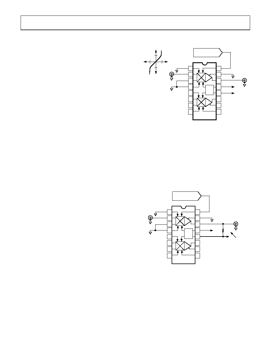
TIME-GAIN CONTROL (TGC) AND TIME-VARIABLE
GAIN (TVG)
Ultrasound and sonar systems share a similar requirement: both
need to provide an exponential increase in gain in response to a
linear control voltage, that is, a gain control that is linear in dB.
Figure 33 shows the AD600/AD602 configured for a control
voltage ramp starting at 625 mV and ending at +625 mV for a
gain-control range of 40 dB. The polarity of the gain-control
voltage can be reversed, and the control voltage inputs, C1HI
and C1LO, can be reversed to achieve the same effect. The gain-
control voltage can be supplied by a voltage output DAC, such
as the AD7244, which contains two complete DACs, operates
from ±5 V supplies, has an internal reference of +3 V, and
provides ±3 V of output swing. As such, it is well suited for use
with the AD600/AD602, needing only a few resistors to scale
the output voltage of the DACs to the levels needed by the
AD600/AD602.
REF
A1
A2
C1HI
A1CM
A1OP
VNEG
A2OP
A2CM
C2HI
C1LO
A1HI
A1LO
GAT1
A2LO
A2HI
C2LO
VG
AD600 OR
AD602
GAT2
+5V
–5V
+
–
+
–
VPOS
VOLTAGE-OUTPUT
DAC
A1
GAIN
0dB
40dB
00
538
-03
1
VG
VPOS
VNEG
VIN
Figure 33. The Simplest Application of the X-AMP Is as a TGC or TVG Amplifier
in Ultrasound or Sonar (Only A1 Connections Shown for Simplicity)
INCREASING OUTPUT DRIVE
The AD600/AD602 output stage has limited capability for
negative-load driving capability. For driving loads less than
500 Ω, the load drive can be increased by approximately 5 mA
by connecting a 1 kΩ pull-down resistor from the output to the
negative supply (see Figure 34).
DRIVING CAPACITIVE LOADS
For driving capacitive loads of greater than 5 pF, insert a 10 Ω
resistor between the output and the load. This lowers the
possibility of oscillation.
1k
1
2
3
4
5
16
15
14
13
12
6
7
8
11
10
9
REF
A1
C1HI
A1CM
A1OP
C1LO
A1HI
A1LO
GAT1
GAIN-CONTROL
VOLTAGE
A2
A2OP
A2CM
C2HI
A2LO
A2HI
C2LO
GAT2
+5V
–5V
+
–
+
–
AD600/
AD602
PULL-DOW
RESISTOR
ADDED
N
00
538
-032
Figure 34. Adding a 1 kΩ Pull-Down Resistor Increases the X-AMP Output
Drive by About 5 mA (Only A1 Connections Shown for Simplicity)
相关PDF资料 |
PDF描述 |
|---|---|
| P50E-040P1-RR1-TG | CONN PLUG 40POS R/A .050" GOL |
| P50E-030P1-SR1-TG | CONN PLUG 30POS R/A .050" GOL |
| 100NH1M | FUSE 100A 690V CLASS AM |
| P50E-026P1-S1-TG | CONN PLUG 26POS STR .050" GOL |
| TV02W141-G | TVS 200W 140V UNIDIRECT SOD-123 |
相关代理商/技术参数 |
参数描述 |
|---|---|
| AD602J | 制造商:AD 制造商全称:Analog Devices 功能描述:Dual, Low Noise, Wideband Variable Gain Amplifiers |
| AD602JCHIPS | 制造商:AD 制造商全称:Analog Devices 功能描述:Dual, Low Noise, Wideband Variable Gain Amplifiers |
| AD602JN | 制造商:Analog Devices 功能描述:SP Amp Variable Gain Amp Dual 制造商:Rochester Electronics LLC 功能描述:VARIABLE GAIN AMP. IC - Bulk 制造商:Analog Devices 功能描述:IC VARIABLE GAIN AMP DIP16 602 |
| AD602JNZ | 功能描述:IC AMP VGA DUAL LN 50MA 16DIP RoHS:是 类别:集成电路 (IC) >> Linear - Amplifiers - Instrumentation 系列:X-AMP® 标准包装:1 系列:- 放大器类型:通用 电路数:4 输出类型:满摆幅 转换速率:0.028 V/µs 增益带宽积:105kHz -3db带宽:- 电流 - 输入偏压:3nA 电压 - 输入偏移:100µV 电流 - 电源:3.3µA 电流 - 输出 / 通道:12mA 电压 - 电源,单路/双路(±):2.7 V ~ 12 V,±1.35 V ~ 6 V 工作温度:-40°C ~ 85°C 安装类型:表面贴装 封装/外壳:14-TSSOP(0.173",4.40mm 宽) 供应商设备封装:14-TSSOP 包装:剪切带 (CT) 其它名称:OP481GRUZ-REELCT |
| AD602JR | 功能描述:IC AMP VGA DUAL LN 50MA 16SOIC RoHS:否 类别:集成电路 (IC) >> Linear - Amplifiers - Instrumentation 系列:X-AMP® 标准包装:2,500 系列:Excalibur™ 放大器类型:J-FET 电路数:1 输出类型:- 转换速率:45 V/µs 增益带宽积:10MHz -3db带宽:- 电流 - 输入偏压:20pA 电压 - 输入偏移:490µV 电流 - 电源:1.7mA 电流 - 输出 / 通道:48mA 电压 - 电源,单路/双路(±):4.5 V ~ 38 V,±2.25 V ~ 19 V 工作温度:-40°C ~ 85°C 安装类型:表面贴装 封装/外壳:8-SOIC(0.154",3.90mm 宽) 供应商设备封装:8-SOIC 包装:带卷 (TR) |
发布紧急采购,3分钟左右您将得到回复。