参数资料
| 型号: | AD602JRZ-R7 |
| 厂商: | Analog Devices Inc |
| 文件页数: | 19/33页 |
| 文件大小: | 0K |
| 描述: | IC AMP VGA DUAL LN 50MA 16SOIC |
| 标准包装: | 400 |
| 系列: | X-AMP® |
| 放大器类型: | 可变增益 |
| 电路数: | 2 |
| 转换速率: | 275 V/µs |
| -3db带宽: | 35MHz |
| 电流 - 输入偏压: | 350nA |
| 电流 - 电源: | 11mA |
| 电流 - 输出 / 通道: | 50mA |
| 电压 - 电源,单路/双路(±): | ±4.75 V ~ 5.25 V |
| 工作温度: | 0°C ~ 70°C |
| 安装类型: | 表面贴装 |
| 封装/外壳: | 16-SOIC(0.295",7.50mm 宽) |
| 供应商设备封装: | 16-SOIC W |
| 包装: | 带卷 (TR) |
第1页第2页第3页第4页第5页第6页第7页第8页第9页第10页第11页第12页第13页第14页第15页第16页第17页第18页当前第19页第20页第21页第22页第23页第24页第25页第26页第27页第28页第29页第30页第31页第32页第33页
AD600/AD602
Rev. F | Page 25 of 3
5
3
–5
4
2
0
1
–1
–3
–2
–4
LOGA
R
IT
H
M
IC
OU
T
P
U
T
(
V
)
1
10
1
100m
10m
1m
100
INPUT SIGNAL (V rms)
2
0
53
8-
05
0
–2.0
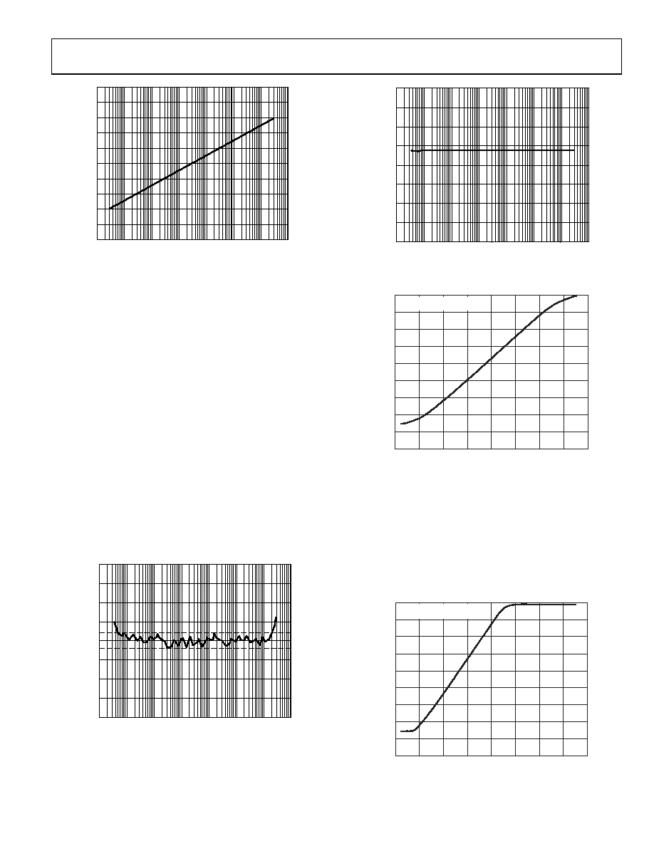
Figure 52. VLOG Is Linear over the Full 120 dB Range
Figure 53 shows the error ripple due to the individual gain
functions bounded by ±0.2 dB (dotted lines) from 6 μV to 2 V.
The small perturbations at about 200 μV and 20 mV, caused by
the impracticality of matching the gain functions perfectly, are
the only sign that the gains are now sequential. Figure 54 is a
plot of VAGC that remains very close to its set value of 316 mV rms
over the full 120 dB range.
To compare the SNRs in the simultaneous and sequential
modes of operation more directly, all interstage attenuation was
input of U1A was shorted, R5 was selected to provide a 20 kHz
bandwidth (R5 = 7.87 kΩ), and only the gain control was
varied, using an external source. The rms value of the noise was
then measured at VOUT and expressed as an SNR relative to
0 dBV, which is almost the maximum output capability of the
AD600. Results for the simultaneous mode can be seen in
Figure 55. The SNR degrades uniformly as the gain is increased.
Note that, because the inverting gain control was used, the gain
in this curve and in Figure 56 decreases for more positive values
of the gain-control voltage.
2.0
0.5
1.0
1.5
–1.5
–1.0
–0.5
GA
IN
E
R
OR
(
d
B
)
–0.2
0.2
0
1
10
1
100m
10m
1m
100
INPUT SIGNAL (V rms)
00
53
8-
0
5
400
300
200
350
250
G
A
IN
ER
R
O
R
(m
V)
1
10
1
100m
10m
1m
100
INPUT SIGNAL (V rms)
1
00
53
8
-05
2
90
0
833.2
20
10
–625.0
–833.2
30
40
50
60
70
80
625.0
416.6
208.3
0
–208.3
–416.6
VC (mV)
S
NR
(
d
B)
Figure 53. Error Ripple Caused by the Individual Gain Functions
Figure 54. VAGC Remains Close to Its Setpoint of
316 mV rms over the Full 120 dB Range
VC SCALE = 10.417mV/dB
90
30
40
50
60
70
80
S
NR
(
d
B)
0
05
38-
053
Figure 55. SNR vs. Control Voltage for Parallel Gain Control (See Figure 47)
In contrast, the SNR for the sequential mode is shown in Figure 56.
U1A always acts as a fixed noise source; varying its gain has no
influence on the output noise. This is a feature of the X-AMP
technique. Therefore, for the first 40 dB of control range
(actually slightly more, as is explained later), when only this
VCA section has its gain varied, the SNR remains constant.
During this time, the gains of U1B and U2A are at their
minimum value of 1.07 dB.
VC (V)
0
3.817
20
10
–0.558
–1.183
3.192
2.567
1.942
1.317
0.692
0.067
00
53
8-
0
5
4
VC SCALE = 31.25mV/dB
Figure 56. SNR vs. Control Voltage for Sequential Gain Control (See Figure 51)
相关PDF资料 |
PDF描述 |
|---|---|
| P4KE75CA-G | TVS 400W 75V 5% BIDIR DO-41 |
| 225CJ | FUSE 225A 600V CERAM BODY CSA |
| AD600JRZ-R7 | IC AMP VGA DUAL LN 50MA 16SOIC |
| AD585JPZ-REEL7 | IC AMP SAMPLE HOLD 50MA 20PLCC |
| NPS 2-T126 5.000 OHM 1% | RES 5.0 OHM 25W 1% DPAK |
相关代理商/技术参数 |
参数描述 |
|---|---|
| AD602JRZ-RL | 功能描述:IC AMP VGA DUAL LN 50MA 16SOIC RoHS:是 类别:集成电路 (IC) >> Linear - Amplifiers - Instrumentation 系列:X-AMP® 标准包装:2,500 系列:Excalibur™ 放大器类型:J-FET 电路数:1 输出类型:- 转换速率:45 V/µs 增益带宽积:10MHz -3db带宽:- 电流 - 输入偏压:20pA 电压 - 输入偏移:490µV 电流 - 电源:1.7mA 电流 - 输出 / 通道:48mA 电压 - 电源,单路/双路(±):4.5 V ~ 38 V,±2.25 V ~ 19 V 工作温度:-40°C ~ 85°C 安装类型:表面贴装 封装/外壳:8-SOIC(0.154",3.90mm 宽) 供应商设备封装:8-SOIC 包装:带卷 (TR) |
| AD602SQ/883B | 制造商:Rochester Electronics LLC 功能描述:VARIABLE GAIN AMP IC - Bulk |
| AD603 | 制造商:AD 制造商全称:Analog Devices 功能描述:Low Noise, 90 MHz Variable Gain Amplifier |
| AD603_05 | 制造商:AD 制造商全称:Analog Devices 功能描述:Low Noise, 90 MHz Variable Gain Amplifier |
发布紧急采购,3分钟左右您将得到回复。