参数资料
| 型号: | AD604AR-REEL |
| 厂商: | Analog Devices Inc |
| 文件页数: | 8/33页 |
| 文件大小: | 0K |
| 描述: | IC AMP VGA DUAL ULN 40MA 24SOIC |
| 标准包装: | 1,000 |
| 系列: | X-AMP® |
| 放大器类型: | 可变增益 |
| 电路数: | 2 |
| 转换速率: | 170 V/µs |
| -3db带宽: | 40MHz |
| 电流 - 输入偏压: | 400nA |
| 电流 - 电源: | 32mA |
| 电流 - 输出 / 通道: | 40mA |
| 工作温度: | -40°C ~ 85°C |
| 安装类型: | 表面贴装 |
| 封装/外壳: | 24-SOIC(0.295",7.50mm 宽) |
| 供应商设备封装: | 24-SOIC W |
| 包装: | 带卷 (TR) |
| 配用: | AD604-EVALZ-ND - BOARD EVAL FOR AD604 AMP |
第1页第2页第3页第4页第5页第6页第7页当前第8页第9页第10页第11页第12页第13页第14页第15页第16页第17页第18页第19页第20页第21页第22页第23页第24页第25页第26页第27页第28页第29页第30页第31页第32页第33页
AD604
Rev. G | Page 15 of 32
The larger portion of the input referred voltage noise comes
from the amplifier with 0.63 nV/√Hz. The current noise is
independent of gain and depends only on the bias current in
the input stage of the preamplifier, which is 3 pA/√Hz.
A unique circuit technique is used to interpolate continuously
among the tap points, thereby providing continuous attenuation
from 0 dB to 48.36 dB. The ladder network, together with the
interpolation mechanism, can be considered a voltage-controlled
potentiometer.
The preamplifier can drive 40 Ω (the nominal feedback resistors)
and the following 175 Ω ladder load of the DSX with low
distortion. For example, at 10 MHz and 1 V at the output, the
preamplifier has less than 45 dB of second and third harmonic
distortion when driven from a low (25 Ω) source resistance.
Because the DSX circuit uses a single voltage power supply, the
input biasing is provided by the VOCM buffer driving the MID
node (see Figure 41). Without internal biasing, the user would
have to dc bias the inputs externally. If not done carefully, the
biasing network can introduce additional noise and offsets. By
providing internal biasing, the user is relieved of this task and
only needs to ac-couple the signal into the DSX. Note that the
input to the DSX is still fully differential if driven differentially;
that is, Pin +DSXx and Pin DSXx see the same signal but with
opposite polarity (see the Ultralow Noise, Differential Input-
Differential Output VGA section).
In applications that require more than 48 dB of gain range, two
AD604 channels can be cascaded. Because the preamplifier has
a limited input signal range and consumes over half (120 mW)
of the total power (220 mW), and its ultralow noise is not necessary
after the first AD604 channel, a shutdown mechanism that
disables only the preamplifier is provided. To shut down the
preamplifier, connect the COM1 pin and/or COM2 pin to the
positive supply; the DSX is unaffected. For additional details,
refer to the Applications Information section.
What changes is the load seen by the driver; it is 175 Ω when
each input is driven single-ended but 350 Ω when driven
differentially. This is easily explained by thinking of the ladder
network as two 175 Ω resistors connected back-to-back with
the middle node, MID, being biased by the VOCM buffer. A
differential signal applied between the +DSXx and DSXx
nodes results in zero current into the MID node, but a single-
ended signal applied to either input, +DSXx or –DSXx, while
the other input is ac-grounded causes the current delivered by
the source to flow into the VOCM buffer via the MID node.
12
11
10
9
8
1
2
3
4
7
6
5
13
16
15
14
24
23
22
21
20
19
18
17
AD604
–DSX1
+DSX1
PAI1
FBK1
PAO1
COM1
COM2
PAI2
FBK2
PAO2
+DSX2
–DSX2
VGN1
VREF
VPOS
GND1
OUT1
VNEG
VPOS
GND2
OUT2
VOCM
VGN2
00
54
0-
04
0
The ladder resistor value of 175 Ω provides the optimum
balance between the load driving capability of the preamplifier
and the noise contribution of the resistors. An advantage of the
X-AMP architecture is that the output referred noise is constant
vs. gain over most of the gain range. Figure 41 shows that the
tap resistance is equal for all taps after only a few taps away
from the inputs. The resistance seen looking into each tap is
54.4 Ω, which makes 0.95 nV/√Hz of Johnson noise spectral
density. Because there are two attenuators, the overall noise
contribution of the ladder network is √2 times 0.95 nV/√Hz
or 1.34 nV/√Hz, a large fraction of the total DSX noise. The
balance of the DSX circuit components contributes another
1.2 nV/√Hz, which together with the attenuator produces
1.8 nV/√Hz of total DSX input referred noise.
Figure 40. Shutdown of Preamplifiers Only
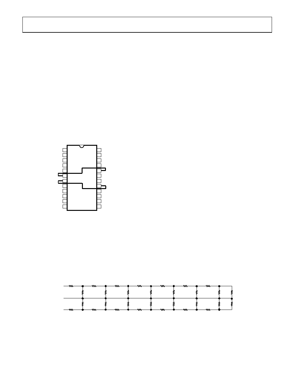
DIFFERENTIAL LADDER (ATTENUATOR)
The attenuator before the fixed-gain amplifier of the DSX is
realized by a differential 7-stage R-1.5R resistive ladder network
with an untrimmed input resistance of 175 Ω single-ended or
350 Ω differential. The signal applied at the input of the ladder
network is attenuated by 6.908 dB per tap; thus, the attenuation
at the first tap is 0 dB, at the second, 13.816 dB, and so on, all
the way to the last tap where the attenuation is 48.356 dB
(see Figure 41).
R
–6.908dB
R
1.5R
RR
–13.82dB
–20.72dB
–27.63dB
–34.54dB
–41.45dB
–48.36dB
+DSXx
MID
–DSXx
NOTES
1. R = 96
2. 1.5R = 144
R
1.5R
175
00
54
0-
04
1
Figure 41. R-1.5R Dual Ladder Network
相关PDF资料 |
PDF描述 |
|---|---|
| 2510-60K2UB | CONN HEADER 10POS STR GOLD T/H |
| 3432-1302UG | CONN HEADER 40POS R/A LONG LATCH |
| 98414-G06-24U | MINITEK SHROUDED HDR TMT |
| 3432-1202 | CONN HEADER 40PS R/A SHORT LATCH |
| 180905-5 | CONN RCPT HSG .250 1POS BLACK |
相关代理商/技术参数 |
参数描述 |
|---|---|
| AD604ARS | 制造商:Analog Devices 功能描述:SP Amp Variable Gain Amp Dual 24-Pin SSOP Tube 制造商:Analog Devices 功能描述:SEMICONDUCTOR ((NW)) |
| AD604ARS-REEL | 制造商:Analog Devices 功能描述:SP Amp Variable Gain Amp Dual 24-Pin SSOP T/R |
| AD604ARS-REEL7 | 制造商:Analog Devices 功能描述:SP Amp Variable Gain Amp Dual 24-Pin SSOP T/R |
| AD604ARSZ | 功能描述:IC AMP VGA DUAL ULN 40MA 24SSOP RoHS:是 类别:集成电路 (IC) >> Linear - Amplifiers - Instrumentation 系列:X-AMP® 标准包装:1 系列:- 放大器类型:通用 电路数:4 输出类型:满摆幅 转换速率:0.028 V/µs 增益带宽积:105kHz -3db带宽:- 电流 - 输入偏压:3nA 电压 - 输入偏移:100µV 电流 - 电源:3.3µA 电流 - 输出 / 通道:12mA 电压 - 电源,单路/双路(±):2.7 V ~ 12 V,±1.35 V ~ 6 V 工作温度:-40°C ~ 85°C 安装类型:表面贴装 封装/外壳:14-TSSOP(0.173",4.40mm 宽) 供应商设备封装:14-TSSOP 包装:剪切带 (CT) 其它名称:OP481GRUZ-REELCT |
| AD604ARSZ-R7 | 功能描述:IC AMP VGA DUAL ULN 40MA 24SSOP RoHS:是 类别:集成电路 (IC) >> Linear - Amplifiers - Instrumentation 系列:X-AMP® 标准包装:2,500 系列:Excalibur™ 放大器类型:J-FET 电路数:1 输出类型:- 转换速率:45 V/µs 增益带宽积:10MHz -3db带宽:- 电流 - 输入偏压:20pA 电压 - 输入偏移:490µV 电流 - 电源:1.7mA 电流 - 输出 / 通道:48mA 电压 - 电源,单路/双路(±):4.5 V ~ 38 V,±2.25 V ~ 19 V 工作温度:-40°C ~ 85°C 安装类型:表面贴装 封装/外壳:8-SOIC(0.154",3.90mm 宽) 供应商设备封装:8-SOIC 包装:带卷 (TR) |
发布紧急采购,3分钟左右您将得到回复。