参数资料
| 型号: | AD605BRZ-RL |
| 厂商: | Analog Devices Inc |
| 文件页数: | 7/25页 |
| 文件大小: | 0K |
| 描述: | IC AMP VGA DUAL LN 40MA 16SOIC |
| 标准包装: | 2,500 |
| 系列: | X-AMP® |
| 放大器类型: | 可变增益 |
| 电路数: | 2 |
| 转换速率: | 170 V/µs |
| -3db带宽: | 40MHz |
| 电流 - 输入偏压: | 400nA |
| 电流 - 电源: | 18mA |
| 电流 - 输出 / 通道: | 40mA |
| 电压 - 电源,单路/双路(±): | 4.5 V ~ 5.5 V |
| 工作温度: | -40°C ~ 85°C |
| 安装类型: | 表面贴装 |
| 封装/外壳: | 16-SOIC(0.154",3.90mm 宽) |
| 供应商设备封装: | 16-SOIC |
| 包装: | 带卷 (TR) |
AD605
Rev. F | Page 14 of 24
1.5R
R
RR
R
–6.908dB
–13.82dB
–20.72dB
–27.63dB
–34.54dB
–41.45dB
–48.36dB
+IN
MID
–IN
NOTE: R = 96
1.5R = 144
175
00
54
1-
0
37
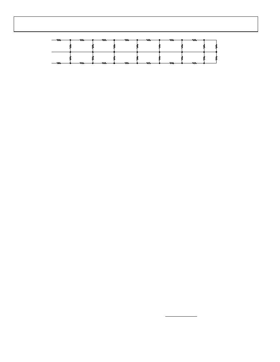
Figure 36. R-1.5R Dual Ladder Network
DIFFERENTIAL LADDER (ATTENUATOR)
The attenuator before the fixed gain amplifier is realized by a
differential, 7-stage, R-1.5R resistive ladder network with an
untrimmed input resistance of 175 Ω single ended or 350 Ω
differentially. The signal applied at the input of the ladder
network is attenuated by 6.908 dB per tap; therefore, the
attenuation at the first tap is 6.908 dB, at the second, 13.816 dB,
and so on all the way to the last tap where the attenuation is
48.356 dB (see Figure 36). A unique circuit technique is used to
interpolate continuously between the tap points, thereby providing
continuous attenuation from 0 dB to 48.36 dB. One can think
of the ladder network together with the interpolation mechanism
as a voltage-controlled potentiometer.
Because the DSX is a single-supply circuit, some means of
biasing its inputs must be provided. Node MID together with
the VOCM buffer performs this function. Without internal
biasing, external biasing is required. If not done carefully, the
biasing network can introduce additional noise and offsets. By
providing internal biasing, the user is relieved of this task and
only needs to ac couple the signal into the DSX. It should be
made clear again that the input to the DSX is still fully differential if
driven differentially, that is, Pin +IN and Pin IN see the same
signal but with opposite polarity. What changes is the load seen
by the driver; it is 175 Ω when each input is driven single ended,
but 350 Ω when driven differentially. This can be easily explained
when thinking of the ladder network as two 175 Ω resistors
connected back-to-back with the middle node, MID, being
biased by the VOCM buffer. A differential signal applied between
nodes +IN and IN results in zero current into Node MID, but
a single-ended signal applied to either input +IN or IN, while the
other input is ac grounded, causes the current delivered by the
source to flow into the VOCM buffer via Node MID.
A feature of the X-AMP architecture is that the output-referred
noise is constant vs. gain over most of the gain range. Referring
to Figure 36, the tap resistance is approximately equal for all
taps within the ladder, excluding the end sections. The resistance
seen looking into each tap is 54.4 Ω, which makes 0.95 nV/√Hz of
Johnson noise spectral density. Because there are two attenuators,
the overall noise contribution of the ladder network is √2 times
0.95 nV/√Hz or 1.34 nV/√Hz, a large fraction of the total DSX
noise. The rest of the DSX circuit components contribute another
1.20 nV/√Hz, which together with the attenuator produces
1.8 nV/√Hz of total DSX input referred noise.
AC COUPLING
The DSX is a single-supply circuit; therefore, its inputs need to
be ac-coupled to accommodate ground-based signals. External
Capacitor C1 and Capacitor C2 in Figure 35 level-shift the input
signal from ground to the dc value established by VOCM (nominal
2.5 V). C1 and C2, together with the 175 Ω looking into each of
DSX inputs (+IN and IN), act as high-pass filters with corner
frequencies depending on the values chosen for C1 and C2. For
example, if C1 and C2 are 0.1 μF, together with the 175 Ω input
resistance of each side of the differential ladder of the DSX, a 3 dB
high-pass corner at 9.1 kHz is formed.
If the DSX output needs to be ground referenced, another ac
coupling capacitor is required for level shifting. This capacitor also
eliminates any dc offsets contributed by the DSX. With a nominal
load of 500 Ω and a 0.1 μF coupling capacitor, this adds a high-pass
filter with 3 dB corner frequency at about 3.2 kHz.
The choice for all three of these coupling capacitors depends on
the application. They should allow the signals of interest to pass
unattenuated, while at the same time, they can be used to limit
the low frequency noise in the system.
GAIN CONTROL INTERFACE
The gain control interface provides an input resistance of
approximately 2 MΩ at Pin VGN1 and gain scaling factors from
20 dB/V to 40 dB/V for VREF input voltages of 2.5 V to 1.25 V,
respectively. The gain varies linearly in decibels for the center
40 dB of gain range, that is, for VGN equal to 0.4 V to 2.4 V for
the 20 dB/V scale and 0.25 V to 1.25 V for the 40 dB/V scale.
Figure 37 shows the ideal gain curves when the FBK-to-OUT
connection is shorted as described by the following equations:
G (20 dB/V) = 20 × VGN 19, VREF = 2.500 V
(3)
G (30 dB/V) = 30 × VGN 19, VREF = 1.6666 V
(4)
G (40 dB/V) = 40 × VGN 19, VREF = 1.250 V
(5)
The equations show that all gain curves intercept at the same
19 dB point; this intercept is 14 dB higher (5 dB) if the FBK-
to-OUT connection is left open. Outside the central linear
range, the gain starts to deviate from the ideal control law but
still provides another 8.4 dB of range. For a given gain scaling,
one can calculate VREF as
Scale
Gain
V
REF
dB/V
20
V
2.500
×
=
(6)
相关PDF资料 |
PDF描述 |
|---|---|
| AD606JR | IC AMP LOG LP 1.2MA 16SOIC |
| AD620AN | IC AMP INST LP LN 18MA 8DIP |
| AD621BRZ | IC AMP INST LDRIFT LP 18MA 8SOIC |
| AD622ARZ-RL | IC AMP INST LP 18MA 8SOIC |
| AD623AR-REEL7 | IC AMP INST R-R LP 8SOIC |
相关代理商/技术参数 |
参数描述 |
|---|---|
| AD605BRZ-RL7 | 制造商:AD 制造商全称:Analog Devices 功能描述:Dual, Low Noise, Single-Supply Variable Gain Amplifier |
| AD605-EB | 制造商:Analog Devices 功能描述: |
| AD605EHDK42GMS | 制造商:Advanced Micro Devices 功能描述:EB E64 4C 605E AM3 45W - Trays |
| AD605-EVALZ | 功能描述:BOARD EVALUATION FOR AD605 RoHS:是 类别:编程器,开发系统 >> 评估板 - 运算放大器 系列:X-AMP® 产品培训模块:Lead (SnPb) Finish for COTS Obsolescence Mitigation Program 标准包装:1 系列:- |
| AD606 | 制造商:AD 制造商全称:Analog Devices 功能描述:50 MHz, 80 dB Demodulating Logarithmic Amplifier with Limiter Output |
发布紧急采购,3分钟左右您将得到回复。