参数资料
| 型号: | AD620AR-REEL7 |
| 厂商: | Analog Devices Inc |
| 文件页数: | 8/21页 |
| 文件大小: | 0K |
| 描述: | IC AMP INST LP LN 18MA 8SOIC |
| 设计资源: | Low Cost Programmable Gain Instrumentation Amplifier Circuit Using ADG1611 and AD620 (CN0146) |
| 标准包装: | 750 |
| 放大器类型: | 仪表 |
| 电路数: | 1 |
| 转换速率: | 1.2 V/µs |
| -3db带宽: | 1MHz |
| 电流 - 输入偏压: | 500pA |
| 电压 - 输入偏移: | 30µV |
| 电流 - 电源: | 900µA |
| 电流 - 输出 / 通道: | 18mA |
| 电压 - 电源,单路/双路(±): | 4.6 V ~ 36 V,±2.3 V ~ 18 V |
| 工作温度: | -40°C ~ 85°C |
| 安装类型: | 表面贴装 |
| 封装/外壳: | 8-SOIC(0.154",3.90mm 宽) |
| 供应商设备封装: | 8-SO |
| 包装: | 带卷 (TR) |
| 其它名称: | AD620AR-REEL7TR |
AD620
Rev. H | Page 15 of 20
Precision V-I Converter
The AD620, along with another op amp and two resistors,
makes a precision current source (Figure 40). The op amp
buffers the reference terminal to maintain good CMR. The
output voltage, VX, of the AD620 appears across R1, which
converts it to a current. This current, less only the input bias
current of the op amp, then flows out to the load.
AD620
RG
–VS
VIN+
VIN–
LOAD
R1
I
L
Vx
I =
L
R1
=
IN+
[(V
) – (V
)] G
IN–
R1
6
5
+ V –
X
4
2
1
8
3
7
+VS
AD705
00775-0-044
Figure 40. Precision Voltage-to-Current Converter (Operates on 1.8 mA, ±3 V)
GAIN SELECTION
The AD620 gain is resistor-programmed by RG, or more
precisely, by whatever impedance appears between Pins 1 and 8.
The AD620 is designed to offer accurate gains using 0.1% to 1%
Note that for G = 1, the RG pins are unconnected (RG = ∞). For
any arbitrary gain, RG can be calculated by using the formula:
1
4
.
49
Ω
=
G
k
R
G
To minimize gain error, avoid high parasitic resistance in series
with RG; to minimize gain drift, RG should have a low TC—less
than 10 ppm/°C—for the best performance.
Table 5. Required Values of Gain Resistors
1% Std Table
Value of RG(Ω)
Calculated
Gain
0.1% Std Table
Value of RG(Ω )
Calculated
Gain
49.9 k
1.990
49.3 k
2.002
12.4 k
4.984
12.4 k
4.984
5.49 k
9.998
5.49 k
9.998
2.61 k
19.93
2.61 k
19.93
1.00 k
50.40
1.01 k
49.91
499
100.0
499
100.0
249
199.4
249
199.4
100
495.0
98.8
501.0
49.9
991.0
49.3
1,003.0
INPUT AND OUTPUT OFFSET VOLTAGE
The low errors of the AD620 are attributed to two sources,
input and output errors. The output error is divided by G when
referred to the input. In practice, the input errors dominate at
high gains, and the output errors dominate at low gains. The
total VOS for a given gain is calculated as
Total Error RTI = input error + (output error/G)
Total Error RTO = (input error × G) + output error
REFERENCE TERMINAL
The reference terminal potential defines the zero output voltage
and is especially useful when the load does not share a precise
ground with the rest of the system. It provides a direct means of
injecting a precise offset to the output, with an allowable range
of 2 V within the supply voltages. Parasitic resistance should be
kept to a minimum for optimum CMR.
INPUT PROTECTION
The AD620 safely withstands an input current of ±60 mA for
several hours at room temperature. This is true for all gains and
power on and off, which is useful if the signal source and
amplifier are powered separately. For longer time periods, the
input current should not exceed 6 mA.
For input voltages beyond the supplies, a protection resistor
should be placed in series with each input to limit the current to
6 mA. These can be the same resistors as those used in the RFI
filter. High values of resistance can impact the noise and AC
CMRR performance of the system. Low leakage diodes (such as
the BAV199) can be placed at the inputs to reduce the required
protection resistance.
AD620
R
REF
R
+SUPPLY
–SUPPLY
VOUT
+IN
–IN
0077
5-
0-
0
52
Figure 41. Diode Protection for Voltages Beyond Supply
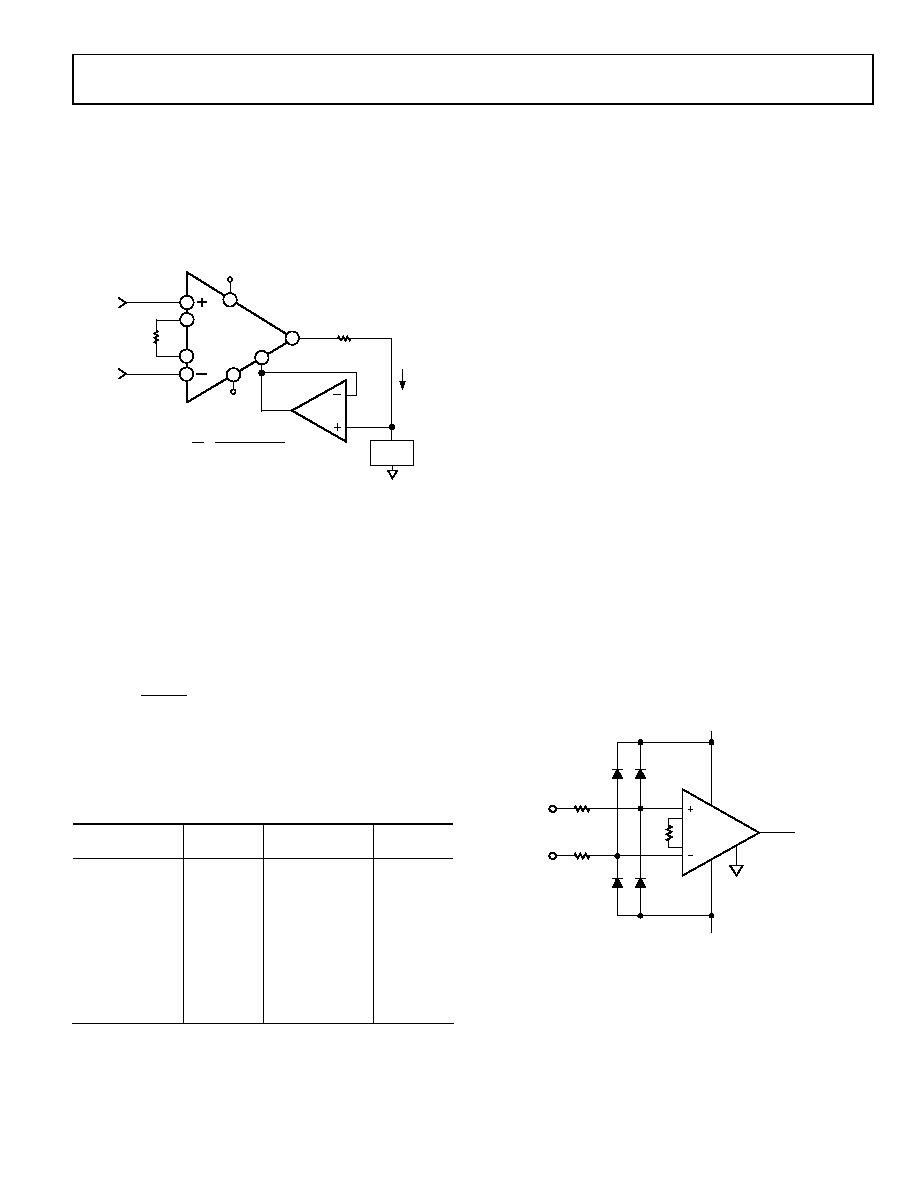
RF INTERFERENCE
All instrumentation amplifiers rectify small out of band signals.
The disturbance may appear as a small dc voltage offset. High
frequency signals can be filtered with a low pass R-C network
placed at the input of the instrumentation amplifier. Figure 42
demonstrates such a configuration. The filter limits the input
相关PDF资料 |
PDF描述 |
|---|---|
| 39804000000 | FUSE T-LAG PROTECT 400MA 65V MP |
| LT1028CSW#TR | IC OP AMP LOW NOISE HS 16SOIC |
| RPC2010JT39R0 | RES PULSE 39 OHM 0.75W 5% 2010 |
| 39805000000 | FUSE T-LAG PROTECT 500MA 65V MP |
| 52963-1 | CONN SPADE SPRING SHORT 12-10AWG |
相关代理商/技术参数 |
参数描述 |
|---|---|
| AD620ARZ | 功能描述:IC AMP INST LP LN 18MA 8SOIC RoHS:是 类别:集成电路 (IC) >> Linear - Amplifiers - Instrumentation 系列:- 标准包装:2,500 系列:- 放大器类型:通用 电路数:4 输出类型:- 转换速率:0.6 V/µs 增益带宽积:1MHz -3db带宽:- 电流 - 输入偏压:45nA 电压 - 输入偏移:2000µV 电流 - 电源:1.4mA 电流 - 输出 / 通道:40mA 电压 - 电源,单路/双路(±):3 V ~ 32 V,±1.5 V ~ 16 V 工作温度:0°C ~ 70°C 安装类型:表面贴装 封装/外壳:14-TSSOP(0.173",4.40mm 宽) 供应商设备封装:14-TSSOP 包装:带卷 (TR) 其它名称:LM324ADTBR2G-NDLM324ADTBR2GOSTR |
| AD620ARZ-REEL | 功能描述:IC AMP INST LP LN 18MA 8SOIC RoHS:是 类别:集成电路 (IC) >> Linear - Amplifiers - Instrumentation 系列:- 标准包装:73 系列:Over-The-Top® 放大器类型:通用 电路数:4 输出类型:满摆幅 转换速率:0.07 V/µs 增益带宽积:200kHz -3db带宽:- 电流 - 输入偏压:1nA 电压 - 输入偏移:285µV 电流 - 电源:50µA 电流 - 输出 / 通道:25mA 电压 - 电源,单路/双路(±):2 V ~ 44 V,±1 V ~ 22 V 工作温度:-40°C ~ 85°C 安装类型:表面贴装 封装/外壳:16-WFDFN 裸露焊盘 供应商设备封装:16-DFN-EP(5x3) 包装:管件 |
| AD620ARZ-REEL7 | 功能描述:IC AMP INST LP LN 18MA 8SOIC RoHS:是 类别:集成电路 (IC) >> Linear - Amplifiers - Instrumentation 系列:- 产品培训模块:Differential Circuit Design Techniques for Communication Applications 标准包装:1 系列:- 放大器类型:RF/IF 差分 电路数:1 输出类型:差分 转换速率:9800 V/µs 增益带宽积:- -3db带宽:2.9GHz 电流 - 输入偏压:3µA 电压 - 输入偏移:- 电流 - 电源:40mA 电流 - 输出 / 通道:- 电压 - 电源,单路/双路(±):3 V ~ 3.6 V 工作温度:-40°C ~ 85°C 安装类型:表面贴装 封装/外壳:16-VQFN 裸露焊盘,CSP 供应商设备封装:16-LFCSP-VQ 包装:剪切带 (CT) 产品目录页面:551 (CN2011-ZH PDF) 其它名称:ADL5561ACPZ-R7CT |
| AD620ARZ-REEL7-MOOG | 制造商:Analog Devices 功能描述: |
| AD620B | 制造商:AD 制造商全称:Analog Devices 功能描述:Low Cost, Low Power Instrumentation Amplifier |
发布紧急采购,3分钟左右您将得到回复。