参数资料
| 型号: | AD620BRZ-R7 |
| 厂商: | Analog Devices Inc |
| 文件页数: | 9/21页 |
| 文件大小: | 0K |
| 描述: | IC AMP INST LP LN 18MA 8SOIC |
| 设计资源: | Low Cost Programmable Gain Instrumentation Amplifier Circuit Using ADG1611 and AD620 (CN0146) |
| 标准包装: | 750 |
| 放大器类型: | 仪表 |
| 电路数: | 1 |
| 转换速率: | 1.2 V/µs |
| -3db带宽: | 1MHz |
| 电流 - 输入偏压: | 500pA |
| 电压 - 输入偏移: | 15µV |
| 电流 - 电源: | 900µA |
| 电流 - 输出 / 通道: | 18mA |
| 电压 - 电源,单路/双路(±): | 4.6 V ~ 36 V,±2.3 V ~ 18 V |
| 工作温度: | -40°C ~ 85°C |
| 安装类型: | 表面贴装 |
| 封装/外壳: | 8-SOIC(0.154",3.90mm 宽) |
| 供应商设备封装: | 8-SO |
| 包装: | 带卷 (TR) |
AD620
Rev. H | Page 16 of 20
signal according to the following relationship:
)
2
(
2
1
C
D
DIFF
C
R
FilterFreq
+
π
=
C
CM
RC
FilterFreq
π
=
2
1
where CD ≥10CC.
CD affects the difference signal. CC affects the common-mode
signal. Any mismatch in R × CC degrades the AD620 CMRR. To
avoid inadvertently reducing CMRR-bandwidth performance,
make sure that CC is at least one magnitude smaller than CD.
The effect of mismatched CCs is reduced with a larger CD:CC
ratio.
499
Ω
AD620
+
–
VOUT
R
CC
CD
CC
+IN
–IN
REF
–15V
0.1
μ F1 μ F
0
+15V
0.1
μ F1 μ F
0
00775-0-045
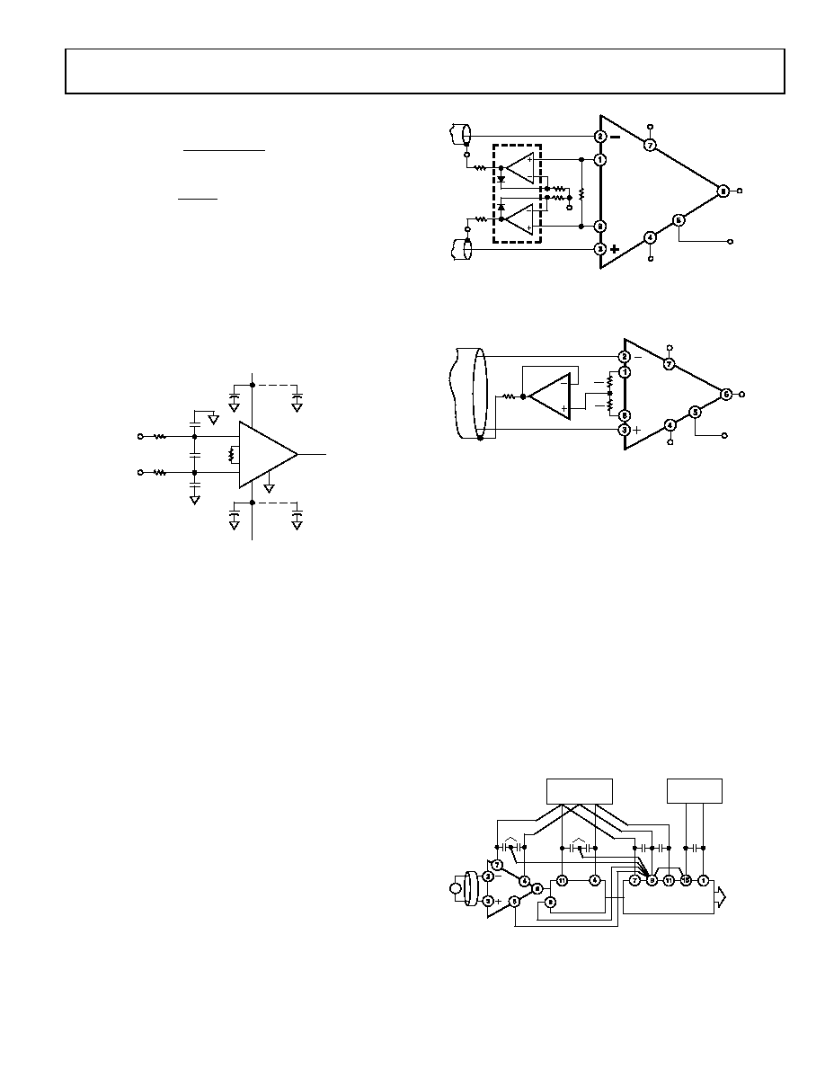
Figure 42. Circuit to Attenuate RF Interference
COMMON-MODE REJECTION
Instrumentation amplifiers, such as the AD620, offer high
CMR, which is a measure of the change in output voltage when
both inputs are changed by equal amounts. These specifications
are usually given for a full-range input voltage change and a
specified source imbalance.
For optimal CMR, the reference terminal should be tied to a
low impedance point, and differences in capacitance and
resistance should be kept to a minimum between the two
inputs. In many applications, shielded cables are used to
minimize noise; for best CMR over frequency, the shield
data guards that are configured to improve ac common-mode
rejections by “bootstrapping” the capacitances of input cable
shields, thus minimizing the capacitance mismatch between the
inputs.
REFERENCE
VOUT
AD620
100
Ω
100
Ω
– INPUT
+ INPUT
AD648
RG
–VS
+VS
–VS
00775-
0-
046
Figure 43. Differential Shield Driver
100
Ω
– INPUT
+ INPUT
REFERENCE
VOUT
AD620
–VS
+VS
2
RG
2
RG
AD548
00775-
0-
047
Figure 44. Common-Mode Shield Driver
GROUNDING
Since the AD620 output voltage is developed with respect to the
potential on the reference terminal, it can solve many
grounding problems by simply tying the REF pin to the
appropriate “local ground.”
To isolate low level analog signals from a noisy digital
environment, many data-acquisition components have separate
analog and digital ground pins (Figure 45). It would be
convenient to use a single ground line; however, current
through ground wires and PC runs of the circuit card can cause
hundreds of millivolts of error. Therefore, separate ground
returns should be provided to minimize the current flow from
the sensitive points to the system ground. These ground returns
must be tied together at some point, usually best at the ADC
package shown in Figure 45.
DIGITAL P.S.
+5V
C
ANALOG P.S.
+15V C –15V
AD574A
DIGITAL
DATA
OUTPUT
+
1
μF
AD620
0.1
μ F
AD585
S/H
ADC
0.1
μ F
1
μF 1μF
00775-
0-
048
Figure 45. Basic Grounding Practice
相关PDF资料 |
PDF描述 |
|---|---|
| GH800 | FUSE 800A 415V INDUST BS IEC |
| AD603ARZ-REEL | IC AMP VGA 90MHZ LN 50MA 8SOIC |
| AD5750BCPZ | IC CURR/VOLT OUT DVR 32LFCSP |
| SM6S20AHE3/2D | TVS 6W 20V 5% SMD DO-218AB |
| SM6S18AHE3/2D | TVS 6W 18V 5% SMD DO-218AB |
相关代理商/技术参数 |
参数描述 |
|---|---|
| AD620BRZ-RL | 功能描述:IC AMP INST LP LN 18MA 8SOIC RoHS:是 类别:集成电路 (IC) >> Linear - Amplifiers - Instrumentation 系列:- 标准包装:150 系列:- 放大器类型:音频 电路数:2 输出类型:- 转换速率:5 V/µs 增益带宽积:12MHz -3db带宽:- 电流 - 输入偏压:100nA 电压 - 输入偏移:500µV 电流 - 电源:6mA 电流 - 输出 / 通道:50mA 电压 - 电源,单路/双路(±):4 V ~ 32 V,±2 V ~ 16 V 工作温度:-40°C ~ 85°C 安装类型:表面贴装 封装/外壳:8-TSSOP(0.173",4.40mm 宽) 供应商设备封装:8-TSSOP 包装:管件 |
| AD620SQ/883B | 功能描述:仪表放大器 IC LOW POWER IN-AMP IC RoHS:否 制造商:Texas Instruments 通道数量: 输入补偿电压:150 V 可用增益调整: 最大输入电阻:10 kOhms 共模抑制比(最小值):88 dB 工作电源电压:2.7 V to 36 V 电源电流:200 uA 最大工作温度:+ 125 C 最小工作温度:- 40 C 封装 / 箱体:MSOP-8 封装:Bulk |
| AD621 | 制造商:AD 制造商全称:Analog Devices 功能描述:10 MHz, 20 V/レs, G = 1, 10, 100, 1000 i CMOS㈢ Programmable Gain Instrumentation Amplifier |
| AD621-00E | 功能描述:SENS MAG SW 20G CROS AXIS 8-MSOP 制造商:nve corp/sensor products 系列:AD 包装:管件 零件状态:有效 功能:全极开关 技术:霍尔效应 极化:任意一种 感应范围:±2.5mT 跳闸,±1.1mT 释放 测试条件:-40°C ~ 125°C 电压 - 电源:4.5 V ~ 30 V 电流 - 电源(最大值):4.5mA 电流 - 输出(最大值):20mA 输出类型:开路集电极 特性:- 工作温度:-40°C ~ 125°C(TA) 封装/外壳:8-TSSOP,8-MSOP(0.118",3.00mm 宽) 供应商器件封装:8-MSOP 标准包装:1,000 |
| AD621-02E | 功能描述:SENSOR MAG SW 20G CROS AXS 8SOIC 制造商:nve corp/sensor products 系列:AD 包装:管件 零件状态:有效 功能:全极开关 技术:霍尔效应 极化:任意一种 感应范围:±2.5mT 跳闸,±1.1mT 释放 测试条件:-40°C ~ 125°C 电压 - 电源:4.5 V ~ 30 V 电流 - 电源(最大值):4.5mA 电流 - 输出(最大值):20mA 输出类型:开路集电极 特性:- 工作温度:-40°C ~ 125°C(TA) 封装/外壳:8-SOIC(0.154",3.90mm 宽) 供应商器件封装:8-SOIC 标准包装:1,000 |
发布紧急采购,3分钟左右您将得到回复。