- 您现在的位置:买卖IC网 > PDF目录5753 > AD621AR-REEL7 (Analog Devices Inc)IC AMP INST LDRIFT LP 18MA 8SOIC PDF资料下载
参数资料
| 型号: | AD621AR-REEL7 |
| 厂商: | Analog Devices Inc |
| 文件页数: | 4/16页 |
| 文件大小: | 0K |
| 描述: | IC AMP INST LDRIFT LP 18MA 8SOIC |
| 标准包装: | 750 |
| 放大器类型: | 仪表 |
| 电路数: | 1 |
| 转换速率: | 1.2 V/µs |
| -3db带宽: | 800kHz |
| 电流 - 输入偏压: | 500pA |
| 电压 - 输入偏移: | 75µV |
| 电流 - 电源: | 900µA |
| 电流 - 输出 / 通道: | 18mA |
| 电压 - 电源,单路/双路(±): | ±2.3 V ~ 18 V |
| 工作温度: | -40°C ~ 85°C |
| 安装类型: | 表面贴装 |
| 封装/外壳: | 8-SOIC(0.154",3.90mm 宽) |
| 供应商设备封装: | 8-SO |
| 包装: | 带卷 (TR) |
AD621
REV. B
–12–
AD548
TO
REF
C
R
TO
VOUT1
–
+
–
+
10
AD621
DAC
0 TO
10V
–
+
VDIFF
0.5V
INPUT A:
10V CM
VCOM
10V–
+
–
+
INPUT B:
1V
OFFSET
VDIFF + VOFFSET
(1.25V + 1V)
VOUT1
G = 10
–
+
10
AD621
VOUT2
TOTAL GAIN = 100
10k
OPTIONAL
USE THIS IN PLACE OF THE DAC FOR ZERO SUPPRESSION FUNCTION.
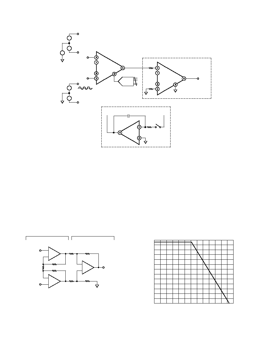
Figure 6. Suppressing a Large Common-Mode or Offset Voltage in Order to Measure a Small Differential Signal
(VS =
±15 V)
The AD621, as well as many other monolithic instrumentation
amplifiers, is based on the “three op amp” in amp circuit (Fig-
ure 7) amplifier. Since the input amplifiers (A1 and A2) have a
common-mode gain of unity and a differential gain equal to the
set gain of the overall in amp, the voltages V1 and V2 are defined
by the equations
V1 = VCM + G
× V
DIFF/2
V2 = VCM – G
× V
DIFF/2
The common-mode voltage will drive the outputs of amplifiers
A1 and A2 to the differential-signal voltage, multiplied by the
gain, spreads them apart. For a 10 V common-mode 0.1 V
differential input, V1 would be at 10.5 V and V2 at 9.5 V.
A1
A3
–
+
10k
A2
–
+
20k
+
–
V1
V2
INPUT AMPLIFIER
DIFFERENTIAL GAIN = 10
COMMON MODE GAIN = 1
OUTPUT AMPLIFIER
DIFFERENTIAL GAIN = 1
COMMON MODE GAIN = 1/1000
4.44k
Figure 7. Typical Three Op Amp Instrumentation
Amplifier, Differential Gain = 10
The AD621’s input amplifiers can provide output voltage within
2.5 V of the supplies. To avoid saturation of the input amplifier
the input voltage must therefore obey the equations:
VCM + G
× V
DIFF/2
≤ (Upper Supply – 2.5 V)
VCM – G
× V
DIFF/2
≥ (Lower Supply + 2.5 V)
Figure 8 shows the trade-off between common-mode and
differential-mode input for
±15 V supplies and G = 10.
By cascading with use of the optional AD621, the circuit of
Figure 6 will provide
±1 V of zero suppression at gains of 10
and 100 (at VOUT1 and VOUT2 respectively) with maximum TCs
of
±4 ppm/°C and ±8 ppm/°C, respectively. Therefore, depend-
ing on the magnitude of the differential input signal, either
VOUT1 or VOUT2 may be used as the output.
VCM – Volts
1.2
0.2
010
2
V
DIFF
–
Volts
48
1.0
0.8
0.6
0.4
6
0
12
Figure 8. Trade-Off Between VCM and VDIFF Range (VS =
±15 V, G = 10), for Reference Pin at Ground
相关PDF资料 |
PDF描述 |
|---|---|
| SL1021B300RS | GAS TUBE GDT 10KA 300V RAD +FS |
| SL1021B250RS | GAS TUBE GDT 10KA 250V RAD +FS |
| 0447005.YXP | FUSE 350V MINI T HOLE EBF 5A |
| 0447010.YXP | FUSE 350V MINI T HOLE EBF 10A |
| 044707.5YXP | FUSE 350V MINI T HOLE EBF 7.5A |
相关代理商/技术参数 |
参数描述 |
|---|---|
| AD621ARZ | 功能描述:IC AMP INST LDRIFT LP 18MA 8SOIC RoHS:是 类别:集成电路 (IC) >> Linear - Amplifiers - Instrumentation 系列:- 标准包装:2,500 系列:- 放大器类型:通用 电路数:4 输出类型:- 转换速率:0.6 V/µs 增益带宽积:1MHz -3db带宽:- 电流 - 输入偏压:45nA 电压 - 输入偏移:2000µV 电流 - 电源:1.4mA 电流 - 输出 / 通道:40mA 电压 - 电源,单路/双路(±):3 V ~ 32 V,±1.5 V ~ 16 V 工作温度:0°C ~ 70°C 安装类型:表面贴装 封装/外壳:14-TSSOP(0.173",4.40mm 宽) 供应商设备封装:14-TSSOP 包装:带卷 (TR) 其它名称:LM324ADTBR2G-NDLM324ADTBR2GOSTR |
| AD621ARZ | 制造商:Analog Devices 功能描述:Instrumentation Amplifier |
| AD621ARZ-R7 | 功能描述:IC AMP INST LDRIFT LP 18MA 8SOIC RoHS:是 类别:集成电路 (IC) >> Linear - Amplifiers - Instrumentation 系列:- 标准包装:150 系列:- 放大器类型:音频 电路数:2 输出类型:- 转换速率:5 V/µs 增益带宽积:12MHz -3db带宽:- 电流 - 输入偏压:100nA 电压 - 输入偏移:500µV 电流 - 电源:6mA 电流 - 输出 / 通道:50mA 电压 - 电源,单路/双路(±):4 V ~ 32 V,±2 V ~ 16 V 工作温度:-40°C ~ 85°C 安装类型:表面贴装 封装/外壳:8-TSSOP(0.173",4.40mm 宽) 供应商设备封装:8-TSSOP 包装:管件 |
| AD621ARZ-RL | 功能描述:IC AMP INST LDRIFT LP 18MA 8SOIC RoHS:是 类别:集成电路 (IC) >> Linear - Amplifiers - Instrumentation 系列:- 标准包装:150 系列:- 放大器类型:音频 电路数:2 输出类型:- 转换速率:5 V/µs 增益带宽积:12MHz -3db带宽:- 电流 - 输入偏压:100nA 电压 - 输入偏移:500µV 电流 - 电源:6mA 电流 - 输出 / 通道:50mA 电压 - 电源,单路/双路(±):4 V ~ 32 V,±2 V ~ 16 V 工作温度:-40°C ~ 85°C 安装类型:表面贴装 封装/外壳:8-TSSOP(0.173",4.40mm 宽) 供应商设备封装:8-TSSOP 包装:管件 |
| AD621B | 制造商:AD 制造商全称:Analog Devices 功能描述:Low Drift, Low Power Instrumentation Amplifier |
发布紧急采购,3分钟左右您将得到回复。