参数资料
| 型号: | AD623ARZ |
| 厂商: | Analog Devices Inc |
| 文件页数: | 13/24页 |
| 文件大小: | 0K |
| 描述: | IC AMP INST R-R LP 8SOIC |
| 产品培训模块: | Instrumentation Amplifiers Performance |
| 标准包装: | 98 |
| 放大器类型: | 仪表 |
| 电路数: | 1 |
| 输出类型: | 满摆幅 |
| 转换速率: | 0.3 V/µs |
| -3db带宽: | 800kHz |
| 电流 - 输入偏压: | 17nA |
| 电压 - 输入偏移: | 25µV |
| 电流 - 电源: | 375µA |
| 电压 - 电源,单路/双路(±): | 2.7 V ~ 12 V,± 2.5 V ~ 6 V |
| 工作温度: | -40°C ~ 85°C |
| 安装类型: | 表面贴装 |
| 封装/外壳: | 8-SOIC(0.154",3.90mm 宽) |
| 供应商设备封装: | 8-SO |
| 包装: | 管件 |
| 产品目录页面: | 770 (CN2011-ZH PDF) |
AD623
Rev. D | Page 20 of 24
Amplifying Signals with Low Common-Mode Voltage
Because the common-mode input range of the AD623 extends
0.1 V below ground, it is possible to measure small differential
signals which have low, or no, common-mode component.
Figure 54 shows a thermocouple application where one side
of the J-type thermocouple is grounded.
5V
0.1F
AD623
RG
1.02k
REF
J-TYPE
THERMOCOUPLE
OUTPUT
2V
00
77
8-
05
3
Figure 54. Amplifying Bipolar Signals with Low Common-Mode Voltage
Over a temperature range of 200°C to +200°C, the J-type thermo-
couple delivers a voltage ranging from 7.890 mV to +10.777 mV.
A programmed gain on the AD623 of 100 (RG = 1.02 kΩ) and a
voltage on the REF pin of 2 V, results in the output voltage ranging
from 1.110 V to 3.077 V relative to ground.
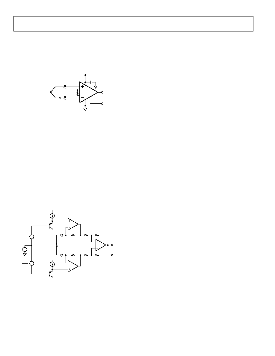
INPUT DIFFERENTIAL AND COMMON-MODE RANGE
vs. SUPPLY AND GAIN
Figure 55 shows a simplified block diagram of the AD623. The
voltages at the outputs of Amplifier A1 and Amplifier A2 are
given by
VA2
= VCM + VDIFF/2 + 0.6 V + VDIFF × RF/RG
= VCM + 0.6 V + VDIFF × Gain/2
VA1
= VCM + VDIFF/2 + 0.6 V + VDIFF × RF/RG
= VCM + 0.6 V VDIFF × Gain/2
POSITIVE SUPPLY
7
4
INVERTING
2
7
4
NEGATIVE SUPPLY
NONINVERTING
3
RF
50k
RF
50k
OUTPUT
6
REF
5
8
1
GAIN
RG
A1
A2
A3
VDIFF
2
–
+
VDIFF
2
–
+
VCM
00778-
054
Figure 55. Simplified Block Diagram
The voltages on these internal nodes are critical in determining
whether the output voltage will be clipped. The VA1 and VA2
voltages can swing from approximately 10 mV above the negative
supply (V or ground) to within approximately 100 mV of the
positive rail before clipping occurs. Based on this and from
the previous equations, the maximum and minimum input
common-mode voltages are given by the following equations:
VCMMAX
= V+ 0.7 V VDIFF × Gain/2
VCMMIN
= V 0.590 V + VDIFF × Gain/2
These equations can be rearranged to give the maximum
possible differential voltage (positive or negative) for a
particular common-mode voltage, gain, and power supply.
Because the signals on A1 and A2 can clip on either rail, the
maximum differential voltage are the lesser of the two equations.
|VDIFFMAX| = 2 (V+ 0.7 V VCM/Gain
|VDIFFMAX| = 2 (VCM V +0.590 V/Gain
However, the range on the differential input voltage range is
also constrained by the output swing. Therefore, the range of
VDIFF may have to be lower according the following equation.
Input Range
≤ Available Output Swing/Gain
For a bipolar input voltage with a common-mode voltage that is
roughly half way between the rails, VDIFFMAX is half the value that
the previous equations yield because the REF pin is at midsupply.
Note that the available output swing is given for different supply
conditions in the Specifications section.
The equations can be rearranged to give the maximum gain for
a fixed set of input conditions. Again, the maximum gain will be
the lesser of the two equations.
GainMAX
= 2 (V+ 0.7 V VCM)/VDIFF
GainMAX
= 2 (VCM V +0.590 V)/VDIFF
Again, it is recommended that the resulting gain times the input
range is less than the available output swing. If this is not the
case, the maximum gain is given by
GainMAX
= Available Output Swing/Input Range
Also for bipolar inputs (that is, input range = 2 VDIFF), the
maximum gain is half the value yielded by the previous equations
because the REF pin must be at midsupply.
The maximum gain and resulting output swing for different
input conditions is given in Table 8. Output voltages are
referenced to the voltage on the REF pin.
For the purposes of computation, it is necessary to break down the
input voltage into its differential and common-mode component.
Therefore, when one of the inputs is grounded or at a fixed
voltage, the common-mode voltage changes as the differential
voltage changes. Take the case of the thermocouple amplifier
in Figure 54. The inverting input on the AD623 is grounded;
therefore, when the input voltage is 10 mV, the voltage on the
noninverting input is 10 mV. For the purpose of the signal swing
calculations, this input voltage should be composed of a common-
mode voltage of 5 mV (that is, (+IN + IN)/2) and a differential
input voltage of 10 mV (that is, +IN IN).
相关PDF资料 |
PDF描述 |
|---|---|
| AD623ARMZ | IC AMP INST R-R LP 8MSOP |
| LTC2055HMS8#PBF | IC OPAMP DUAL ZERO DRFT LP 8MSOP |
| LTC6103IMS8#PBF | IC AMP CURRENT SENSE 8-MSOP |
| AWHW40-G-SMD-R | CONN HEADER LO-PRO 40POS AU SMD |
| LT6402CUD-20#PBF | IC DIFF AMP/ADC DRVR 16-QFN |
相关代理商/技术参数 |
参数描述 |
|---|---|
| AD623ARZ | 制造商:Analog Devices 功能描述:IC INSTR AMP 800KHZ 110DB 8SOIC 制造商:Analog Devices 功能描述:IC, INSTR AMP, 800KHZ, 110DB, 8SOIC |
| AD623ARZ-R7 | 功能描述:IC AMP INST R-R LP 8SOIC RoHS:是 类别:集成电路 (IC) >> Linear - Amplifiers - Instrumentation 系列:- 标准包装:1,000 系列:- 放大器类型:电压反馈 电路数:4 输出类型:满摆幅 转换速率:33 V/µs 增益带宽积:20MHz -3db带宽:30MHz 电流 - 输入偏压:2nA 电压 - 输入偏移:3000µV 电流 - 电源:2.5mA 电流 - 输出 / 通道:30mA 电压 - 电源,单路/双路(±):4.5 V ~ 16.5 V,±2.25 V ~ 8.25 V 工作温度:-40°C ~ 85°C 安装类型:表面贴装 封装/外壳:14-SOIC(0.154",3.90mm 宽) 供应商设备封装:14-SOIC 包装:带卷 (TR) |
| AD623ARZ-RL | 功能描述:IC AMP INST R-R LP 8SOIC RoHS:是 类别:集成电路 (IC) >> Linear - Amplifiers - Instrumentation 系列:- 标准包装:1,000 系列:- 放大器类型:电压反馈 电路数:4 输出类型:满摆幅 转换速率:33 V/µs 增益带宽积:20MHz -3db带宽:30MHz 电流 - 输入偏压:2nA 电压 - 输入偏移:3000µV 电流 - 电源:2.5mA 电流 - 输出 / 通道:30mA 电压 - 电源,单路/双路(±):4.5 V ~ 16.5 V,±2.25 V ~ 8.25 V 工作温度:-40°C ~ 85°C 安装类型:表面贴装 封装/外壳:14-SOIC(0.154",3.90mm 宽) 供应商设备封装:14-SOIC 包装:带卷 (TR) |
| AD623ARZ-RL7 | 制造商:Analog Devices 功能描述:Rail-to-Rail,InstrumentationAmplifier 制造商:Analog Devices Inc. 功能描述:Rail-to-Rail,InstrumentationAmplifier |
| AD623B | 制造商:AD 制造商全称:Analog Devices 功能描述:Single Supply, Rail-to-Rail, Low Cost Instrumentation Amplifier |
发布紧急采购,3分钟左右您将得到回复。