参数资料
| 型号: | AD623BRZ |
| 厂商: | Analog Devices Inc |
| 文件页数: | 8/24页 |
| 文件大小: | 0K |
| 描述: | IC AMP INST R-R LP 8SOIC |
| 产品培训模块: | Instrumentation Amplifiers Performance |
| 标准包装: | 98 |
| 放大器类型: | 仪表 |
| 电路数: | 1 |
| 输出类型: | 满摆幅 |
| 转换速率: | 0.3 V/µs |
| -3db带宽: | 800kHz |
| 电流 - 输入偏压: | 17nA |
| 电压 - 输入偏移: | 25µV |
| 电流 - 电源: | 375µA |
| 电压 - 电源,单路/双路(±): | 2.7 V ~ 12 V,± 2.5 V ~ 6 V |
| 工作温度: | -40°C ~ 85°C |
| 安装类型: | 表面贴装 |
| 封装/外壳: | 8-SOIC(0.154",3.90mm 宽) |
| 供应商设备封装: | 8-SO |
| 包装: | 管件 |
| 产品目录页面: | 770 (CN2011-ZH PDF) |
AD623
Rev. D | Page 16 of 24
APPLICATIONS INFORMATION
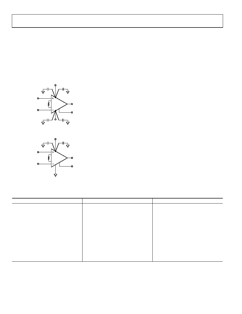
BASIC CONNECTION
the AD623. The +VS and VS terminals are connected to the
power supply. The supply can be either bipolar (VS = ±2.5 V to
±6 V) or single supply (VS = 0 V, +VS = 3.0 V to 12 V). Power
supplies should be capacitively decoupled close to the power pins of
the device. For the best results, use surface-mount 0.1 μF ceramic
chip capacitors and 10 μF electrolytic tantalum capacitors.
0
077
8-
0
42
RG
VIN
OUTPUT
VOUT
REF
RG
REF (INPUT)
+2.5V TO +6V
+VS
10F
0.1F
–2.5V TO –6V
–VS
10F
0.1F
Figure 42. Dual-Supply Basic Connection
00
77
8-
0
55
RG
VIN
OUTPUT
VOUT
REF
RG
REF (INPUT)
+3V TO +12V
+VS
10F
0.1F
Figure 43. Single-Supply Basic Connection
The input voltage, which can be either single-ended (tie either
IN or +IN to ground), or differential is amplified by the
programmed gain. The output signal appears as the voltage
difference between the OUTPUT pin and the externally applied
voltage on the REF input. For a ground-referenced output, REF
should be grounded.
GAIN SELECTION
The gain of the AD623 is resistor programmed by RG, or more
precisely, by whatever impedance appears between Pin 1 and
Pin 8. The AD623 is designed to offer accurate gains using 0.1%
to 1% tolerance resistors. Table 5 shows the required values of
RG for the various gains. Note that for G = 1, the RG terminals
are unconnected (RG = ∞). For any arbitrary gain, RG can be
calculated by
RG
= 100 kΩ/(G 1)
REFERENCE TERMINAL
The reference terminal potential defines the zero output voltage
and is especially useful when the load does not share a precise
ground with the rest of the system. It provides a direct means of
injecting a precise offset to the output. The reference terminal is
also useful when bipolar signals are being amplified because it
can be used to provide a virtual ground voltage. The voltage on
the reference terminal can be varied from VS to +VS.
Table 5. Required Values of Gain Resistors
Desired Gain
1% Standard Table Value of RG (Ω)
Calculated Gain Using 1% Resistors
2
100 k
2
5
24.9 k
5.02
10
11 k
10.09
20
5.23 k
20.12
33
3.09 k
33.36
40
2.55 k
40.21
50
2.05 k
49.78
65
1.58 k
64.29
100
1.02 k
99.04
200
499
201.4
500
200
501
1000
100
1001
相关PDF资料 |
PDF描述 |
|---|---|
| LT1077ACN8#PBF | IC PREC OP-AMP MICRPWR SNGL 8DIP |
| LT1122CS8#PBF | IC OP-AMP JFET FASTSETTLNG 8SOIC |
| 1N6267ARL4G | TVS ZENER UNIDIR 1500W 6.8V AXL |
| AD8250ARMZ-R7 | IC AMP INST ICMOS LDRIFT 10MSOP |
| AD8251ARMZ-R7 | IC AMP INST ICMOS LDRIFT 10MSOP |
相关代理商/技术参数 |
参数描述 |
|---|---|
| AD623BRZ | 制造商:Analog Devices 功能描述:INST AMP RR 12V 800KHZ 8SOIC |
| AD623BRZ-R7 | 功能描述:IC AMP INST R-R LP 8SOIC RoHS:是 类别:集成电路 (IC) >> Linear - Amplifiers - Instrumentation 系列:- 标准包装:1 系列:- 放大器类型:通用 电路数:4 输出类型:满摆幅 转换速率:0.028 V/µs 增益带宽积:105kHz -3db带宽:- 电流 - 输入偏压:3nA 电压 - 输入偏移:100µV 电流 - 电源:3.3µA 电流 - 输出 / 通道:12mA 电压 - 电源,单路/双路(±):2.7 V ~ 12 V,±1.35 V ~ 6 V 工作温度:-40°C ~ 85°C 安装类型:表面贴装 封装/外壳:14-TSSOP(0.173",4.40mm 宽) 供应商设备封装:14-TSSOP 包装:剪切带 (CT) 其它名称:OP481GRUZ-REELCT |
| AD623BRZ-RL | 功能描述:IC AMP INST R-R LP 8SOIC RoHS:是 类别:集成电路 (IC) >> Linear - Amplifiers - Instrumentation 系列:- 标准包装:1 系列:- 放大器类型:通用 电路数:4 输出类型:满摆幅 转换速率:0.028 V/µs 增益带宽积:105kHz -3db带宽:- 电流 - 输入偏压:3nA 电压 - 输入偏移:100µV 电流 - 电源:3.3µA 电流 - 输出 / 通道:12mA 电压 - 电源,单路/双路(±):2.7 V ~ 12 V,±1.35 V ~ 6 V 工作温度:-40°C ~ 85°C 安装类型:表面贴装 封装/外壳:14-TSSOP(0.173",4.40mm 宽) 供应商设备封装:14-TSSOP 包装:剪切带 (CT) 其它名称:OP481GRUZ-REELCT |
| AD623-EVAL | 制造商:Analog Devices 功能描述:Evaluation Board For The AD623 Converts A Differential Signal To A Single-Ended Signal |
| AD624 | 制造商:AD 制造商全称:Analog Devices 功能描述:10 MHz, 20 V/レs, G = 1, 10, 100, 1000 i CMOS㈢ Programmable Gain Instrumentation Amplifier |
发布紧急采购,3分钟左右您将得到回复。