参数资料
| 型号: | AD624ADZ |
| 厂商: | Analog Devices Inc |
| 文件页数: | 16/17页 |
| 文件大小: | 0K |
| 描述: | IC AMP INST 25MHZ PREC LN 16CDIP |
| 标准包装: | 23 |
| 放大器类型: | 仪表 |
| 电路数: | 1 |
| 转换速率: | 5 V/µs |
| 增益带宽积: | 25MHz |
| -3db带宽: | 1MHz |
| 电流 - 输入偏压: | 50nA |
| 电压 - 输入偏移: | 200µV |
| 电流 - 电源: | 3.5mA |
| 电压 - 电源,单路/双路(±): | ±6 V ~ 18 V |
| 工作温度: | -25°C ~ 85°C |
| 安装类型: | 通孔 |
| 封装/外壳: | 16-CDIP(0.300",7.62mm) |
| 供应商设备封装: | 16-CDIP 侧面铜焊 |
| 包装: | 管件 |
| 产品目录页面: | 770 (CN2011-ZH PDF) |
REV. C
AD624
–7–
AD624
+VS
VOUT
10k
1%
1k
10T
10k
1%
RG1
G = 100
G = 200
G = 500
RG2
–VS
200
0.1%
100k
1%
500
0.1%
1k
0.1%
INPUT
20V p-p
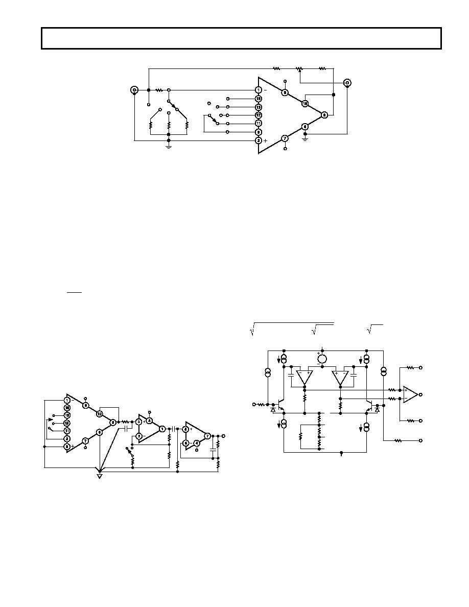
Figure 25. Settling Time Test Circuit
THEORY OF OPERATION
The AD624 is a monolithic instrumentation amplifier based on
a modification of the classic three-op-amp instrumentation
amplifier. Monolithic construction and laser-wafer-trimming
allow the tight matching and tracking of circuit components and
the high level of performance that this circuit architecture is ca-
pable of.
A preamp section (Q1–Q4) develops the programmed gain by
the use of feedback concepts. Feedback from the outputs of A1
and A2 forces the collector currents of Q1–Q4 to be constant
thereby impressing the input voltage across RG.
The gain is set by choosing the value of RG from the equation,
Gain =
40 k
RG
+ 1. The value of RG also sets the transconduct-
ance of the input preamp stage increasing it asymptotically to
the transconductance of the input transistors as RG is reduced
for larger gains. This has three important advantages. First, this
approach allows the circuit to achieve a very high open loop gain
of 3
× 108 at a programmed gain of 1000 thus reducing gain
related errors to a negligible 3 ppm. Second, the gain bandwidth
product which is determined by C3 or C4 and the input trans-
conductance, reaches 25 MHz. Third, the input voltage noise
reduces to a value determined by the collector current of the
input transistors for an RTI noise of 4 nV/
√Hz at G ≥ 500.
AD624
+VS
100
200
RG2
–VS
16.2k
+VS
1/2
AD712
9.09k
G1, 100, 200
1k
1 F
G500
100
1 F
1.62M
–VS
1 F
16.2k
1.82k
500
1/2
AD712
Figure 26. Noise Test Circuit
INPUT CONSIDERATIONS
Under input overload conditions the user will see RG + 100
and two diode drops (~1.2 V) between the plus and minus
inputs, in either direction. If safe overload current under all
conditions is assumed to be 10 mA, the maximum overload
voltage is ~
±2.5 V. While the AD624 can withstand this con-
tinuously, momentary overloads of
±10 V will not harm the
device. On the other hand the inputs should never exceed the
supply voltage.
The AD524 should be considered in applications that require
protection from severe input overload. If this is not possible,
external protection resistors can be put in series with the inputs
of the AD624 to augment the internal (50
) protection resis-
tors. This will most seriously degrade the noise performance.
For this reason the value of these resistors should be chosen to
be as low as possible and still provide 10 mA of current limiting
under maximum continuous overload conditions. In selecting
the value of these resistors, the internal gain setting resistor and
the 1.2 volt drop need to be considered. For example, to pro-
tect the device from a continuous differential overload of 20 V
at a gain of 100, 1.9 k
of resistance is required. The internal
gain resistor is 404
; the internal protect resistor is 100 .
There is a 1.2 V drop across D1 or D2 and the base-emitter
junction of either Q1 and Q3 or Q2 and Q4 as shown in Figure
27, 1400
of external resistance would be required (700 in
series with each input). The RTI noise in this case would be
4 KTRext
+(4 nV / Hz)2 = 6.2 nV / Hz
50
13
50 A
I1
50 A
C3
I2
50 A
R57
20k
R56
20k
500
SENSE
+IN
VO
REF
I4
50 A
200
100
4445
80.2
124
225.3
–IN
–VS
RG1 RG2
C4
VB
A2
R52
10k
R55
10k
A3
R53
10k
R54
10k
+VS
50
Q1, Q3
Q2,
Q4
A1
Figure 27. Simplified Circuit of Amplifier; Gain Is Defined
as (R56 + R57)/(RG) + 1. For a Gain of 1, RG Is an Open
Circuit.
INPUT OFFSET AND OUTPUT OFFSET
Voltage offset specifications are often considered a figure of
merit for instrumentation amplifiers. While initial offset may
be adjusted to zero, shifts in offset voltage due to temperature
variations will cause errors. Intelligent systems can often correct
for this factor with an autozero cycle, but there are many small-
signal high-gain applications that don’t have this capability.
Voltage offset and offset drift each have two components; input
and output. Input offset is that component of offset that is
相关PDF资料 |
PDF描述 |
|---|---|
| AD600JNZ | IC AMP VGA DUAL LN 50MA 16DIP |
| TSW-107-14-S-S | CONN HEADER 7POS .100" SGL GOLD |
| AD604ARZ | IC AMP VGA DUAL ULN 40MA 24SOIC |
| TSW-104-14-G-D | CONN HEADER 8POS .100" DUAL GOLD |
| AD526BDZ | IC AMP PGA 10MA 16CDIP |
相关代理商/技术参数 |
参数描述 |
|---|---|
| AD624B | 制造商:AD 制造商全称:Analog Devices 功能描述:Precision Instrumentation Amplifier |
| AD624BD | 功能描述:IC AMP INST 25MHZ PREC LN 16CDIP RoHS:否 类别:集成电路 (IC) >> Linear - Amplifiers - Instrumentation 系列:- 标准包装:2,500 系列:- 放大器类型:通用 电路数:1 输出类型:满摆幅 转换速率:0.11 V/µs 增益带宽积:350kHz -3db带宽:- 电流 - 输入偏压:4nA 电压 - 输入偏移:20µV 电流 - 电源:260µA 电流 - 输出 / 通道:20mA 电压 - 电源,单路/双路(±):2.7 V ~ 36 V,±1.35 V ~ 18 V 工作温度:-40°C ~ 85°C 安装类型:表面贴装 封装/外壳:8-SOIC(0.154",3.90mm 宽) 供应商设备封装:8-SO 包装:带卷 (TR) |
| AD624BD-G | 制造商:Rochester Electronics LLC 功能描述: |
| AD624BDZ | 功能描述:IC AMP INST 25MHZ PREC LN 16CDIP RoHS:是 类别:集成电路 (IC) >> Linear - Amplifiers - Instrumentation 系列:- 标准包装:2,500 系列:- 放大器类型:通用 电路数:4 输出类型:- 转换速率:0.6 V/µs 增益带宽积:1MHz -3db带宽:- 电流 - 输入偏压:45nA 电压 - 输入偏移:2000µV 电流 - 电源:1.4mA 电流 - 输出 / 通道:40mA 电压 - 电源,单路/双路(±):3 V ~ 32 V,±1.5 V ~ 16 V 工作温度:0°C ~ 70°C 安装类型:表面贴装 封装/外壳:14-TSSOP(0.173",4.40mm 宽) 供应商设备封装:14-TSSOP 包装:带卷 (TR) 其它名称:LM324ADTBR2G-NDLM324ADTBR2GOSTR |
| AD624C | 制造商:AD 制造商全称:Analog Devices 功能描述:Precision Instrumentation Amplifier |
发布紧急采购,3分钟左右您将得到回复。