参数资料
| 型号: | AD624BD |
| 厂商: | Analog Devices Inc |
| 文件页数: | 17/17页 |
| 文件大小: | 0K |
| 描述: | IC AMP INST 25MHZ PREC LN 16CDIP |
| 产品变化通告: | Product Discontinuance 27/Oct/2011 |
| 标准包装: | 1 |
| 放大器类型: | 仪表 |
| 电路数: | 1 |
| 转换速率: | 5 V/µs |
| 增益带宽积: | 25MHz |
| -3db带宽: | 1MHz |
| 电流 - 输入偏压: | 25nA |
| 电压 - 输入偏移: | 75µV |
| 电流 - 电源: | 3.5mA |
| 电压 - 电源,单路/双路(±): | ±6 V ~ 18 V |
| 工作温度: | -25°C ~ 85°C |
| 安装类型: | 通孔 |
| 封装/外壳: | 16-CDIP(0.300",7.62mm) |
| 供应商设备封装: | 16-CDIP 侧面铜焊 |
| 包装: | 管件 |
REV. C
AD624
–8–
directly proportional to gain i.e., input offset as measured at
the output at G = 100 is 100 times greater than at G = 1.
Output offset is independent of gain. At low gains, output offset
drift is dominant, while at high gains input offset drift domi-
nates. Therefore, the output offset voltage drift is normally
specified as drift at G = 1 (where input effects are insignificant),
while input offset voltage drift is given by drift specification at a
high gain (where output offset effects are negligible). All input-
related numbers are referred to the input (RTI) which is to say
that the effect on the output is “G” times larger. Voltage offset
vs. power supply is also specified at one or more gain settings
and is also RTI.
By separating these errors, one can evaluate the total error inde-
pendent of the gain setting used. In a given gain configura-
tion both errors can be combined to give a total error referred to
the input (R.T.I.) or output (R.T.O.) by the following formula:
Total Error R.T.I. = input error + (output error/gain)
Total Error R.T.O. = (Gain
× input error) + output error
As an illustration, a typical AD624 might have a +250
V out-
put offset and a –50
V input offset. In a unity gain configura-
tion, the total output offset would be 200
V or the sum of the
two. At a gain of 100, the output offset would be –4.75 mV
or: +250
V + 100 (–50 V) = –4.75 mV.
The AD624 provides for both input and output offset adjust-
ment. This optimizes nulling in very high precision applications
and minimizes offset voltage effects in switched gain applica-
tions. In such applications the input offset is adjusted first at the
highest programmed gain, then the output offset is adjusted at
G = 1.
GAIN
The AD624 includes high accuracy pretrimmed internal
gain resistors. These allow for single connection program-
ming of gains of 1, 100, 200 and 500. Additionally, a variety
of gains including a pretrimmed gain of 1000 can be achieved
through series and parallel combinations of the internal resis-
tors. Table I shows the available gains and the appropriate
pin connections and gain temperature coefficients.
The gain values achieved via the combination of internal
resistors are extremely useful. The temperature coefficient of the
gain is dependent primarily on the mismatch of the temperature
coefficients of the various internal resistors. Tracking of these
resistors is extremely tight resulting in the low gain TCs shown
in Table I.
If the desired value of gain is not attainable using the inter-
nal resistors, a single external resistor can be used to achieve
any gain between 1 and 10,000. This resistor connected between
AD624
G = 100
RG2
–VS
OUTPUT
SIGNAL
COMMON
VOUT
10k
–INPUT
RG1
G = 200
G = 500
+INPUT
INPUT
OFFSET
NULL
+VS
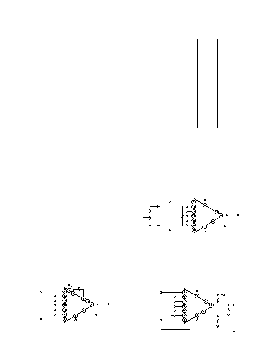
Figure 28. Operating Connections for G = 200
Table I.
Temperature
Gain
Coefficient
Pin 3
(Nominal)
to Pin
Connect Pins
1
–0 ppm/
°C
––
100
–1.5 ppm/
°C13
–
125
–5 ppm/
°C
13
11 to 16
137
–5.5 ppm/
°C
13
11 to 12
186.5
–6.5 ppm/
°C
13
11 to 12 to 16
200
–3.5 ppm/
°C12
–
250
–5.5 ppm/
°C
12
11 to 13
333
–15 ppm/
°C
12
11 to 16
375
–0.5 ppm/
°C
12
13 to 16
500
–10 ppm/
°C11
–
624
–5 ppm/
°C
11
13 to 16
688
–1.5 ppm/
°C
11
11 to 12; 13 to 16
831
+4 ppm/
°C
11
16 to 12
1000
0 ppm/
°C
11
16 to 12; 13 to 11
Pins 3 and 16 programs the gain according to the formula
RG =
40k
G
1
(see Figure 29). For best results RG should be a precision resis-
tor with a low temperature coefficient. An external RG affects both
gain accuracy and gain drift due to the mismatch between it and
the internal thin-film resistors R56 and R57. Gain accuracy is
determined by the tolerance of the external RG and the absolute
accuracy of the internal resistors (
±20%). Gain drift is determined
by the mismatch of the temperature coefficient of RG and the tem-
perature coefficient of the internal resistors (–15 ppm/
°C typ),
and the temperature coefficient of the internal interconnections.
AD624
RG2
–VS
REFERENCE
VOUT
–INPUT
RG1
2.105k
+INPUT
+VS
OR
1.5k
1k
G =
+ 1 = 20
20%
40.000
2.105
Figure 29. Operating Connections for G = 20
The AD624 may also be configured to provide gain in the out-
put stage. Figure 30 shows an H pad attenuator connected to
the reference and sense lines of the AD624. The values of R1,
R2 and R3 should be selected to be as low as possible to mini-
mize the gain variation and reduction of CMRR. Varying R2
will precisely set the gain without affecting CMRR. CMRR is
determined by the match of R1 and R3.
AD624
G = 100
RG2
–VS
VOUT
–INPUT
RG1
G = 200
G = 500
+INPUT
+VS
RL
R3
6k
R2
5k
R1
6k
(R2||20k ) + R1 + R3)
(R2||20k )
G =
(R1 + R2 + R3) || RL
2k
Figure 30. Gain of 2500
相关PDF资料 |
PDF描述 |
|---|---|
| 8-35111-1 | CONN RING 10-12 AWG #5/16 PIDG |
| 1.5KE6.8A | TVS 1500W 6.8V UNIDIRECT AXIAL |
| 1.5KE68A | TVS 1500W 68V UNIDIRECT AXIAL |
| RMCF1210JT150R | RES 150 OHM 1/3W 5% 1210 SMD |
| 1.5KE75A | TVS 1500W 75V UNIDIRECT AXIAL |
相关代理商/技术参数 |
参数描述 |
|---|---|
| AD624BD-G | 制造商:Rochester Electronics LLC 功能描述: |
| AD624BDZ | 功能描述:IC AMP INST 25MHZ PREC LN 16CDIP RoHS:是 类别:集成电路 (IC) >> Linear - Amplifiers - Instrumentation 系列:- 标准包装:2,500 系列:- 放大器类型:通用 电路数:4 输出类型:- 转换速率:0.6 V/µs 增益带宽积:1MHz -3db带宽:- 电流 - 输入偏压:45nA 电压 - 输入偏移:2000µV 电流 - 电源:1.4mA 电流 - 输出 / 通道:40mA 电压 - 电源,单路/双路(±):3 V ~ 32 V,±1.5 V ~ 16 V 工作温度:0°C ~ 70°C 安装类型:表面贴装 封装/外壳:14-TSSOP(0.173",4.40mm 宽) 供应商设备封装:14-TSSOP 包装:带卷 (TR) 其它名称:LM324ADTBR2G-NDLM324ADTBR2GOSTR |
| AD624C | 制造商:AD 制造商全称:Analog Devices 功能描述:Precision Instrumentation Amplifier |
| AD624CD | 功能描述:IC AMP INST 25MHZ PREC LN 16CDIP RoHS:否 类别:集成电路 (IC) >> Linear - Amplifiers - Instrumentation 系列:- 标准包装:2,500 系列:- 放大器类型:通用 电路数:1 输出类型:满摆幅 转换速率:0.11 V/µs 增益带宽积:350kHz -3db带宽:- 电流 - 输入偏压:4nA 电压 - 输入偏移:20µV 电流 - 电源:260µA 电流 - 输出 / 通道:20mA 电压 - 电源,单路/双路(±):2.7 V ~ 36 V,±1.35 V ~ 18 V 工作温度:-40°C ~ 85°C 安装类型:表面贴装 封装/外壳:8-SOIC(0.154",3.90mm 宽) 供应商设备封装:8-SO 包装:带卷 (TR) |
| AD624CDZ | 功能描述:IC AMP INST 25MHZ PREC LN 16CDIP RoHS:是 类别:集成电路 (IC) >> Linear - Amplifiers - Instrumentation 系列:- 标准包装:2,500 系列:- 放大器类型:通用 电路数:4 输出类型:- 转换速率:0.6 V/µs 增益带宽积:1MHz -3db带宽:- 电流 - 输入偏压:45nA 电压 - 输入偏移:2000µV 电流 - 电源:1.4mA 电流 - 输出 / 通道:40mA 电压 - 电源,单路/双路(±):3 V ~ 32 V,±1.5 V ~ 16 V 工作温度:0°C ~ 70°C 安装类型:表面贴装 封装/外壳:14-TSSOP(0.173",4.40mm 宽) 供应商设备封装:14-TSSOP 包装:带卷 (TR) 其它名称:LM324ADTBR2G-NDLM324ADTBR2GOSTR |
发布紧急采购,3分钟左右您将得到回复。