参数资料
| 型号: | AD625CD |
| 厂商: | Analog Devices Inc |
| 文件页数: | 2/15页 |
| 文件大小: | 0K |
| 描述: | IC AMP INST 25MHZ LN 16CDIP |
| 产品变化通告: | Product Discontinuance 27/Oct/2011 |
| 标准包装: | 1 |
| 放大器类型: | 仪表 |
| 电路数: | 1 |
| 转换速率: | 5 V/µs |
| 增益带宽积: | 25MHz |
| -3db带宽: | 650kHz |
| 电流 - 输入偏压: | 10nA |
| 电压 - 输入偏移: | 10µV |
| 电流 - 电源: | 3.5mA |
| 电压 - 电源,单路/双路(±): | ±6 V ~ 18 V |
| 工作温度: | -40°C ~ 85°C |
| 安装类型: | 通孔 |
| 封装/外壳: | 16-CDIP(0.300",7.62mm) |
| 供应商设备封装: | 16-CDIP 侧面铜焊 |
| 包装: | 管件 |
AD625
REV. D
–10–
the I
× R drops “inside the loop” and virtually eliminating this
error source.
Typically, IC instrumentation amplifiers are rated for a full
±10
volt output swing into 2 k
. In some applications, however, the
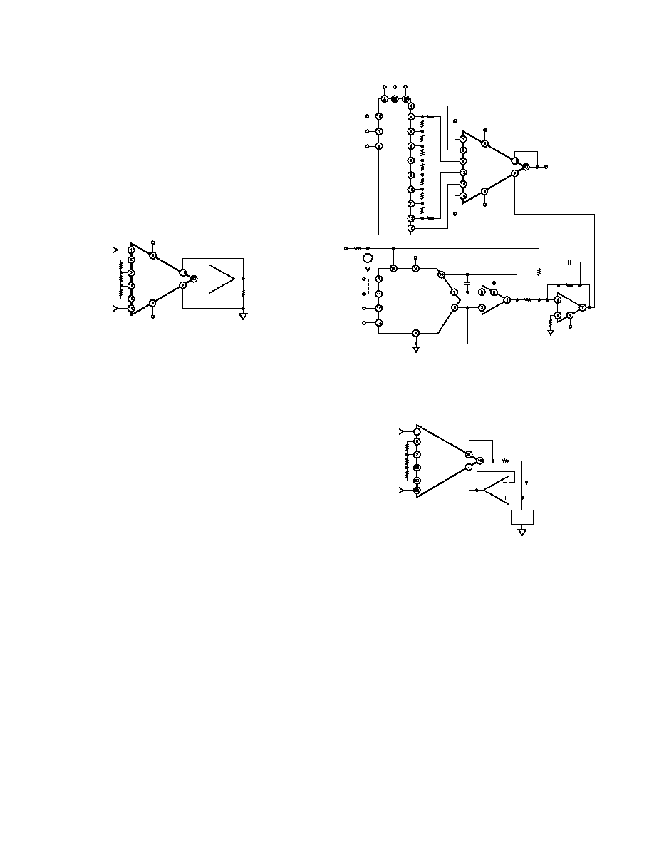
need exists to drive more current into heavier loads. Figure 29
shows how a high-current booster may be connected “inside the
loop” of an instrumentation amplifier. By using an external
power boosting circuit, the power dissipated by the AD625 will
remain low, thereby, minimizing the errors induced by self-
heating. The effects of nonlinearities, offset and gain inaccura-
cies of the buffer are reduced by the loop gain of the AD625’s
output amplifier.
AD625
+VS
–VS
RF
RG
RF
VIN+
VIN–
RI
SENSE
REFERENCE
X1
Figure 29. AD625 /Instrumentation Amplifier with Output
Current Booster
REFERENCE TERMINAL
The reference terminal may be used to offset the output by up
to
±10 V. This is useful when the load is “floating” or does not
share a ground with the rest of the system. It also provides a
direct means of injecting a precise offset. However, it must be
remembered that the total output swing is
±10 volts, from
ground, to be shared between signal and reference offset.
The AD625 reference terminal must be presented with nearly
zero impedance. Any significant resistance, including those
caused by PC layouts or other connection techniques, will in-
crease the gain of the noninverting signal path, thereby, upset-
ting the common-mode rejection of the in-amp. Inadvertent
thermocouple connections created in the sense and reference
lines should also be avoided as they will directly affect the out-
put offset voltage and output offset voltage drift.
In the AD625 a reference source resistance will unbalance the
CMR trim by the ratio of 10 k
/R
REF. For example, if the refer-
ence source impedance is 1
, CMR will be reduced to 80 dB
(10 k
/1 = 80 dB). An operational amplifier may be used to
provide the low impedance reference point as shown in Figure
30. The input offset voltage characteristics of that amplifier will
add directly to the output offset voltage performance of the
instrumentation amplifier.
The circuit of Figure 30 also shows a CMOS DAC operating in
the bipolar mode and connected to the reference terminal to
provide software controllable offset adjustments. The total offset
range is equal to
±(V
REF/2
× R5/R4), however, to be symmetri-
cal about 0 V R3 = 2
× R4.
The offset per bit is equal to the total offset range divided by 2
N,
where N = number of bits of the DAC. The range of offset for
Figure 30 is
±120 mV, and the offset is incremented in steps of
0.9375 mV/LSB.
AD625
+VS
–VS
VOUT
SENSE
AD7502
A0
A1
EN
GND VDD VSS
+IN
–IN
1/2
AD712
1/2
AD712
REFERENCE
VREF
AD589
1.2V
VS 39k
MSB
LSB
DATA
INPUTS
CS
WR
+VS
AD7524
8-BIT DAC
RFB
C1
OUT 1
OUT 2
+VS
R4
10k
R3
20k
5k
–VS
R5
2k
0.01 F
Figure 30. Software Controllable Offset
An instrumentation amplifier can be turned into a voltage-to-
current converter by taking advantage of the sense and reference
terminals as shown in Figure 31.
AD625
RF
RG
RF
VIN+
VIN–
SENSE
IL
AD711
LOAD
+VX–
R1
Figure 31. Voltage-to-Current Converter
By establishing a reference at the “low” side of a current setting
resistor, an output current may be defined as a function of input
voltage, gain and the value of that resistor. Since only a small
current is demanded at the input of the buffer amplifier A1, the
forced current IL will largely flow through the load. Offset and
drift specifications of A2 must be added to the output offset and
drift specifications of the In-Amp.
INPUT AND OUTPUT OFFSET VOLTAGE
Offset voltage specifications are often considered a figure of
merit for instrumentation amplifiers. While initial offset may be
adjusted to zero, shifts in offset voltage due to temperature
variations will cause errors. Intelligent systems can often correct
for this factor with an autozero cycle, but this requires extra
circuitry.
相关PDF资料 |
PDF描述 |
|---|---|
| 8020.0520.PT | FUSE 4A 250VAC AXIAL SLOW |
| TSW-128-17-L-S | CONN HEADER 28POS .100" SGL GOLD |
| AD625BD | IC AMP INST 25MHZ LN 16CDIP |
| 1-52042-0 | CONN RING 6 AWG #10 P-GRIP |
| AD625AD | IC AMP INST 25MHZ LN 16CDIP |
相关代理商/技术参数 |
参数描述 |
|---|---|
| AD625CD/+ | 制造商:未知厂家 制造商全称:未知厂家 功能描述:Instrumentation Amp, Resistor-Programmable |
| AD625CDZ | 功能描述:IC AMP INST 25MHZ LN 16CDIP RoHS:是 类别:集成电路 (IC) >> Linear - Amplifiers - Instrumentation 系列:- 标准包装:1 系列:- 放大器类型:通用 电路数:4 输出类型:满摆幅 转换速率:0.028 V/µs 增益带宽积:105kHz -3db带宽:- 电流 - 输入偏压:3nA 电压 - 输入偏移:100µV 电流 - 电源:3.3µA 电流 - 输出 / 通道:12mA 电压 - 电源,单路/双路(±):2.7 V ~ 12 V,±1.35 V ~ 6 V 工作温度:-40°C ~ 85°C 安装类型:表面贴装 封装/外壳:14-TSSOP(0.173",4.40mm 宽) 供应商设备封装:14-TSSOP 包装:剪切带 (CT) 其它名称:OP481GRUZ-REELCT |
| AD625J | 制造商:AD 制造商全称:Analog Devices 功能描述:Programmable Gain Instrumentation Amplifier |
| AD625JN | 制造商:Analog Devices 功能描述:SP Amp INSTR Amp Single 制造商:Analog Devices 功能描述:IC AMP INSTRUMENTATION DIP16 625 |
| AD625JN/+ | 制造商:未知厂家 制造商全称:未知厂家 功能描述:Instrumentation Amp, Resistor-Programmable |
发布紧急采购,3分钟左右您将得到回复。