参数资料
| 型号: | AD625CDZ |
| 厂商: | Analog Devices Inc |
| 文件页数: | 14/15页 |
| 文件大小: | 0K |
| 描述: | IC AMP INST 25MHZ LN 16CDIP |
| 标准包装: | 1 |
| 放大器类型: | 仪表 |
| 电路数: | 1 |
| 转换速率: | 5 V/µs |
| 增益带宽积: | 25MHz |
| -3db带宽: | 650kHz |
| 电流 - 输入偏压: | 10nA |
| 电压 - 输入偏移: | 10µV |
| 电流 - 电源: | 3.5mA |
| 电压 - 电源,单路/双路(±): | ±6 V ~ 18 V |
| 工作温度: | -40°C ~ 85°C |
| 安装类型: | 通孔 |
| 封装/外壳: | 16-CDIP(0.300",7.62mm) |
| 供应商设备封装: | 16-CDIP 侧面铜焊 |
| 包装: | 管件 |
AD625
REV. D
–8–
THEORY OF OPERATION
The AD625 is a monolithic instrumentation amplifier based on
a modification of the classic three-op-amp approach. Monolithic
construction and laser-wafer-trimming allow the tight matching
and tracking of circuit components. This insures the high level
of performance inherent in this circuit architecture.
A preamp section (Q1–Q4) provides additional gain to A1 and
A2. Feedback from the outputs of A1 and A2 forces the collec-
tor currents of Q1–Q4 to be constant, thereby, impressing the
input voltage across RG. This creates a differential voltage at the
outputs of A1 and A2 which is given by the gain (2RF/RG + 1)
times the differential portion of the input voltage. The unity
gain subtracter, A3, removes any common-mode signal from the
output voltage yielding a single ended output, VOUT, referred to
the potential at the reference pin.
The value of RG is the determining factor of the transconduc-
tance of the input preamp stage. As RG is reduced for larger
gains the transconductance increases. This has three important
advantages. First, this approach allows the circuit to achieve a
very high open-loop gain of (3
× 108 at programmed gains ≥ 500)
thus reducing gain related errors. Second, the gain-bandwidth
product, which is determined by C3, C4, and the input trans-
conductance, increases with gain, thereby, optimizing frequency
response. Third, the input voltage noise is reduced to a value
determined by the collector current of the input transistors
(4 nV/
√Hz).
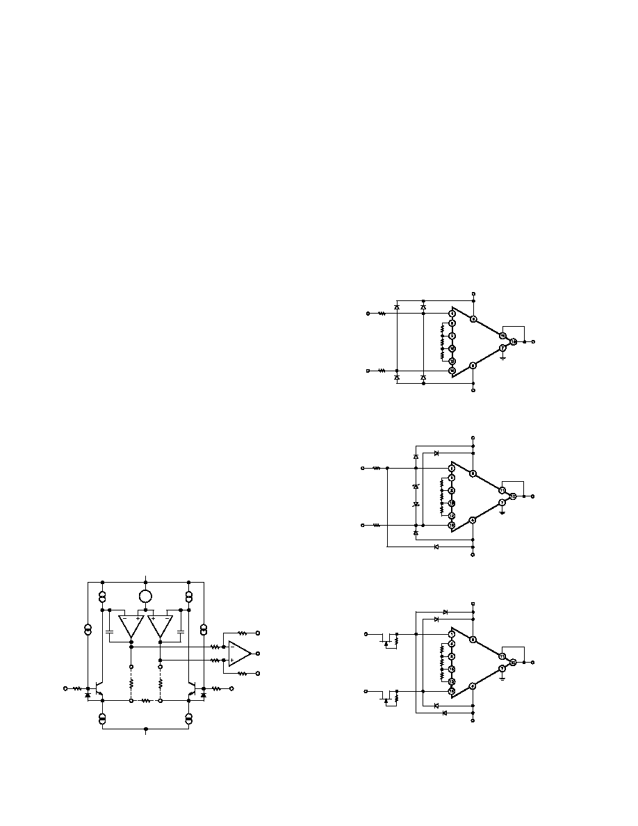
INPUT PROTECTION
Differential input amplifiers frequently encounter input voltages
outside of their linear range of operation. There are two consid-
erations when applying input protection for the AD625; 1) that
continuous input current must be limited to less than 10 mA
and 2) that input voltages must not exceed either supply by
more than one diode drop (approximately 0.6 V @ 25
°C).
Under differential overload conditions there is (RG + 100)
in
series with two diode drops (approximately 1.2 V) between the
plus and minus inputs, in either direction. With no external protec-
tion and RG very small (i.e., 40
), the maximum overload
voltage the AD625 can withstand, continuously, is approximately
±2.5 V. Figure 26a shows the external components necessary to
protect the AD625 under all overload conditions at any gain.
VB
+
–
GAIN
DRIVE
GAIN
DRIVE
RF
RG
50 A50 A
C3
C4
A1
A2
10k
50
GAIN
SENSE
GAIN
SENSE
Q1, Q3
Q2, Q4
50
50 A50 A
10k
–IN
+VS
–VS
+IN
SENSE
VO
REF
Figure 25. Simplified Circuit of the AD625
The diodes to the supplies are only necessary if input voltages
outside of the range of the supplies are encountered. In higher
gain applications where differential voltages are small, back-to-
back Zener diodes and smaller resistors, as shown in Figure
26b, provides adequate protection. Figure 26c shows low cost
FETs with a maximum ON resistance of 300
configured to offer
input protection with minimal degradation to noise, (5.2 nV/
√Hz
compared to normal noise performance of 4 nV/
√Hz).
During differential overload conditions, excess current will flow
through the gain sense lines (Pins 2 and 15). This will have no
effect in fixed gain applications. However, if the AD625 is being
used in an SPGA application with a CMOS multiplexer, this
current should be taken into consideration. The current capa-
bilities of the multiplexer may be the limiting factor in allowable
overflow current. The ON resistance of the switch should be
included as part of RG when calculating the necessary input
protection resistance.
AD625
+VS
–VS
RF
RG
RF
FD333
–IN
+IN
1.4k
VOUT
Figure 26a. Input Protection Circuit
AD625
+VS
–VS
RF
RG
RF
FD333
–IN
+IN
500
VOUT
FD333
1N5837A
500
Figure 26b. Input Protection Circuit for G > 5
AD625
+VS
–VS
RF
RG
RF
FD333
–IN
+IN
VOUT
FD333
2k
2N5952
2k
2N5952
Figure 26c. Input Protection Circuit
相关PDF资料 |
PDF描述 |
|---|---|
| 929647-04-29-I | CONN HEADER .100 SNGL STR 29POS |
| TSW-139-23-G-D | CONN HEADER 78POS .100" DL GOLD |
| PBC24DBEN | CONN HEADER .100 DUAL R/A 48POS |
| 929665-08-16-I | CONN HEADER .100 DUAL STR 32POS |
| 9-146309-0-24 | CONN HEADR BRKWAY .100 48POS R/A |
相关代理商/技术参数 |
参数描述 |
|---|---|
| AD625J | 制造商:AD 制造商全称:Analog Devices 功能描述:Programmable Gain Instrumentation Amplifier |
| AD625JN | 制造商:Analog Devices 功能描述:SP Amp INSTR Amp Single 制造商:Analog Devices 功能描述:IC AMP INSTRUMENTATION DIP16 625 |
| AD625JN/+ | 制造商:未知厂家 制造商全称:未知厂家 功能描述:Instrumentation Amp, Resistor-Programmable |
| AD625JNZ | 功能描述:IC AMP INST 25MHZ LN 16DIP RoHS:是 类别:集成电路 (IC) >> Linear - Amplifiers - Instrumentation 系列:- 标准包装:2,500 系列:- 放大器类型:通用 电路数:4 输出类型:- 转换速率:0.6 V/µs 增益带宽积:1MHz -3db带宽:- 电流 - 输入偏压:45nA 电压 - 输入偏移:2000µV 电流 - 电源:1.4mA 电流 - 输出 / 通道:40mA 电压 - 电源,单路/双路(±):3 V ~ 32 V,±1.5 V ~ 16 V 工作温度:0°C ~ 70°C 安装类型:表面贴装 封装/外壳:14-TSSOP(0.173",4.40mm 宽) 供应商设备封装:14-TSSOP 包装:带卷 (TR) 其它名称:LM324ADTBR2G-NDLM324ADTBR2GOSTR |
| AD625K | 制造商:AD 制造商全称:Analog Devices 功能描述:Programmable Gain Instrumentation Amplifier |
发布紧急采购,3分钟左右您将得到回复。