参数资料
| 型号: | AD625JNZ |
| 厂商: | Analog Devices Inc |
| 文件页数: | 5/15页 |
| 文件大小: | 0K |
| 描述: | IC AMP INST 25MHZ LN 16DIP |
| 标准包装: | 25 |
| 放大器类型: | 仪表 |
| 电路数: | 1 |
| 转换速率: | 5 V/µs |
| 增益带宽积: | 25MHz |
| -3db带宽: | 650kHz |
| 电流 - 输入偏压: | 30nA |
| 电压 - 输入偏移: | 50µV |
| 电流 - 电源: | 3.5mA |
| 电压 - 电源,单路/双路(±): | ±6 V ~ 18 V |
| 工作温度: | 0°C ~ 70°C |
| 安装类型: | 通孔 |
| 封装/外壳: | 16-DIP(0.300",7.62mm) |
| 供应商设备封装: | 16-PDIP |
| 包装: | 管件 |
| 产品目录页面: | 770 (CN2011-ZH PDF) |
AD625
REV. D
–13–
–
VIN
+
12-BIT
DAS
10k
AD625
10k
VS
–INPUT
–GAIN
SENSE
–GAIN
DRIVE
+GAIN
DRIVE
+GAIN
SENSE
+INPUT
20k
15.6k
3.9k
975k
650k
975k
3.9k
20k
15.6k
CS
IS
IOUT
COUT
RON
CS-OUT
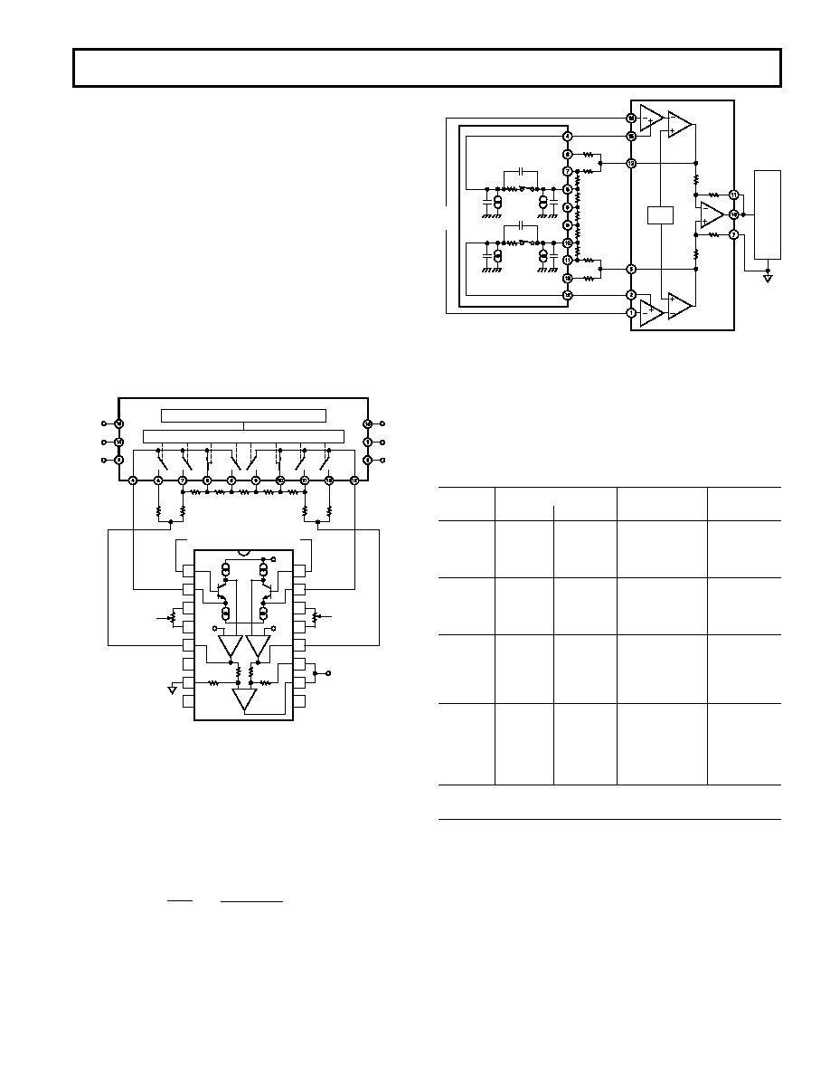
Figure 39. SPGA with Multiplexer Error Sources
Figure 39 shows a complete SPGA feeding a 12-bit DAS with a
0 V–10 V input range. This configuration was used in the error
budget analysis shown in Table II. The gain used for the RTI
calculations is set at 16. As the gain is changed, the ON resis-
tance of the multiplexer and the feedback resistance will change,
which will slightly alter the values in the table.
Table II. Errors Induced by Multiplexer to an SPGA
Induced
Specifications
Voltage Offset
Error
AD625C
AD7520KN
Calculation
Induced RTI
RTI Offset
Gain Sense Switch
40 nA
× 170 =
6.8
V
Voltage
Offset
Resistance
6.8
V
Current
170
40 nA
RTI Offset
Gain Sense Differential
60 nA
× 6.8 =
0.41
V
Voltage
Current
Switch
0.41
V
60 nA
Resistance
6.8
RTO Offset Feedback
Differential
2 (0.2 nA
× 20 k) 0.5 V
Voltage
Resistance
Leakage
= 8
V/16
20 k
1
Current (IS)
2
+0.2 nA
–0.2 nA
RTO Offset Feedback
Differential
2 (1 nA
× 20 k)
2.5
V
Voltage
Resistance
Leakage
= 40
V/16
20 k
1
Current
(IOUT)
2
+1 nA
–1 nA
Total error induced by a typical CMOS multiplexer
to an SPGA at +25
°C
10.21
A
NOTES
1The resistor for this calculation is the user-provided feedback resistance (R
F).
20 k
is recommended value (see Resistor Programmable Gain Amplifier section).
2The leakage currents (I
S and IOUT) will induce an offset voltage, however, the offset
will be determined by the difference between the leakages of each “half’’ of the
differential multiplexer. The differential leakage current is multiplied by the
feedback resistance (see Note 1), to determine offset voltage. Because differential
leakage current is not a parameter specified on multiplexer data sheets, the most
extreme difference (one most positive and one most negative) was used for the
calculations in Table II. Typical performance will be much better.
**The frequency response and settling will be affected by the ON resistance and
internal capacitance of the multiplexer. Figure 40 shows the settling time vs.
ON resistance at different gain settings for an AD625 based SPGA.
**Switch resistance and leakage current errors can be reduced by using relays.
These capacitances may also be incorporated as part of the
external input protection circuit (see section on Input Protec-
tion). As a general practice every effort should be made to
match the extraneous capacitance at Pins 15 and 2, and Pins 1
and 16, to preserve high ac CMR.
SOFTWARE PROGRAMMABLE GAIN AMPLIFIER
An SPGA provides the ability to externally program precision
gains from digital inputs. Historically, the problem in systems
requiring electronic switching of gains has been the ON resis-
tance (RON) of the multiplexer, which appears in series with the
gain setting resistor RG. This can result in substantial gain errors
and gain drifts. The AD625 eliminates this problem by making
the gain drive and gain sense pins available (Pins 2, 15, 5, 12;
see Figure 39). Consequently the multiplexer’s ON resistance is
removed from the signal current path. This transforms the ON
resistance error into a small nullable offset error. To clarify this
point, an error budget analysis has been performed in Table II
based on the SPGA configuration shown in Figure 39.
+GAIN
SENSE
+INPUT
–INPUT
RTI NULL
+VS
+GAIN DRIVE
–GAIN DRIVE
NC
REF
–VS
VOUT
+VS
A1
A2
AD625
10k
A3
1
2
3
4
5
6
7
8
16
15
14
13
12
11
10
9
–GAIN
SENSE
TTL/DTL TO CMOS LEVEL TRANSLATOR
DECODER/DRIVER
3.9k
975
650
975
3.9k
15.6k
20k
AD7502
A0
A1
EN
VSS
VDD
GND
–VS
RTO NULL
Figure 38. SPGA in a Gain of 16
Figure 38 shows an AD625 based SPGA with possible gains of
1, 4, 16, 64. RG equals the resistance between the gain sense
lines (Pins 2 and 15) of the AD625. In Figure 38, RG equals
the sum of the two 975
resistors and the 650 resistor, or
2600
. RF equals the resistance between the gain sense and the
gain drive pins (Pins 12 and 15, or Pins 2 and 5), that is RF
equals the 15.6 k
resistor plus the 3.9 k resistor, or 19.5 k.
The gain, therefore equals:
2RF
RG
+1=
2(19.5 k
)
(2.6 k
)
+1=16
As the switches of the differential multiplexer proceed synchro-
nously, RG and RF change, resulting in the various programmed
gain settings.
相关PDF资料 |
PDF描述 |
|---|---|
| LT1101AIN8#PBF | IC PREC INSTRMNT-AMP SNGL 8-DIP |
| RMCF0603JT75R0 | RES 75 OHM 1/10W 5% 0603 SMD |
| 0791081064 | CONN RCPT 2MM GOLD DL 30CKT |
| 0901471312 | C-GRID PCB CONN SR VT AU-F 12POS |
| RMCF0603JT4M70 | RES 4.7M OHM 1/10W 5% 0603 SMD |
相关代理商/技术参数 |
参数描述 |
|---|---|
| AD625K | 制造商:AD 制造商全称:Analog Devices 功能描述:Programmable Gain Instrumentation Amplifier |
| AD625KN | 制造商:Analog Devices 功能描述:SP Amp INSTR Amp Single 制造商:Analog Devices 功能描述:IC AMP INSTRUMENTATION |
| AD625KNZ | 功能描述:IC AMP INST 25MHZ LN 16DIP RoHS:是 类别:集成电路 (IC) >> Linear - Amplifiers - Instrumentation 系列:- 标准包装:2,500 系列:- 放大器类型:通用 电路数:4 输出类型:- 转换速率:0.6 V/µs 增益带宽积:1MHz -3db带宽:- 电流 - 输入偏压:45nA 电压 - 输入偏移:2000µV 电流 - 电源:1.4mA 电流 - 输出 / 通道:40mA 电压 - 电源,单路/双路(±):3 V ~ 32 V,±1.5 V ~ 16 V 工作温度:0°C ~ 70°C 安装类型:表面贴装 封装/外壳:14-TSSOP(0.173",4.40mm 宽) 供应商设备封装:14-TSSOP 包装:带卷 (TR) 其它名称:LM324ADTBR2G-NDLM324ADTBR2GOSTR |
| AD625KNZ | 制造商:Analog Devices 功能描述:IC AMP GAIN |
| AD625S | 制造商:AD 制造商全称:Analog Devices 功能描述:Programmable Gain Instrumentation Amplifier |
发布紧急采购,3分钟左右您将得到回复。