参数资料
| 型号: | AD627ARZ-R7 |
| 厂商: | Analog Devices Inc |
| 文件页数: | 9/25页 |
| 文件大小: | 0K |
| 描述: | IC AMP INST R-R 25MA 8SOIC |
| 产品培训模块: | Power Line Monitoring Instrumentation Amplifiers Performance |
| 标准包装: | 1 |
| 放大器类型: | 仪表 |
| 电路数: | 1 |
| 输出类型: | 满摆幅 |
| 转换速率: | 0.06 V/µs |
| -3db带宽: | 80kHz |
| 电流 - 输入偏压: | 2nA |
| 电压 - 输入偏移: | 25µV |
| 电流 - 电源: | 60µA |
| 电流 - 输出 / 通道: | 25mA |
| 电压 - 电源,单路/双路(±): | 2.2 V ~ 36 V,±1.1 V ~ 18 V |
| 工作温度: | -40°C ~ 85°C |
| 安装类型: | 表面贴装 |
| 封装/外壳: | 8-SOIC(0.154",3.90mm 宽) |
| 供应商设备封装: | 8-SO |
| 包装: | 标准包装 |
| 产品目录页面: | 771 (CN2011-ZH PDF) |
| 其它名称: | AD627ARZ-R7DKR |
AD627
Data Sheet
Rev. E | Page 16 of 24
Table 6. Recommended Values of Gain Resistors
Desired Gain
1% Standard Table
Value of RG
Resulting Gain
5
∞
5.00
6
200 kΩ
6.00
7
100 kΩ
7.00
8
68.1 kΩ
7.94
9
51.1 kΩ
8.91
10
40.2 kΩ
9.98
15
20 kΩ
15.00
20
13.7 kΩ
19.60
25
10 kΩ
25.00
30
8.06 kΩ
29.81
40
5.76 kΩ
39.72
50
4.53 kΩ
49.15
60
3.65 kΩ
59.79
70
3.09 kΩ
69.72
80
2.67 kΩ
79.91
90
2.37 kΩ
89.39
100
2.1 kΩ
100.24
200
1.05 kΩ
195.48
500
412 Ω
490.44
1000
205 Ω
980.61
REFERENCE TERMINAL
The reference terminal potential defines the zero output voltage
and is especially useful when the load does not share a precise
ground with the rest of the system. It provides a direct means of
injecting a precise offset to the output. The reference terminal is
also useful when amplifying bipolar signals, because it provides
a virtual ground voltage.
The AD627 output voltage is developed with respect to the poten-
tial on the reference terminal; therefore, tying the REF pin to the
appropriate local ground solves many grounding problems. For
optimal CMR, tie the REF pin to a low impedance point.
INPUT RANGE LIMITATIONS IN SINGLE-SUPPLY
APPLICATIONS
In general, the maximum achievable gain is determined by the
available output signal range. However, in single-supply applica-
tions where the input common-mode voltage is nearly or equal
to 0, some limitations on the gain can be set. Although the
Specifications section nominally defines the input, output, and
reference pin ranges, the voltage ranges on these pins are
mutually interdependent. Figure 37 shows the simplified
that has a common-mode component, VCM. The voltage on the
A1 op amp output is a function of VDIFF, VCM, the voltage on the
REF pin, and the programmed gain. This voltage is given by
VA1 = 1.25 (VCM + 0.5 V) 0.25 VREF VDIFF (25 k/RG + 0.625) (3)
The voltage on A1 can also be expressed as a function of the
actual voltages on the –IN and +IN pins (V and V+) such that
VA1 = 1.25 ((V) + 0.5 V) 0.25 VREF ((V+) (V)) 25 k/RG (4)
The output of A1 is capable of swinging to within 50 mV of the
negative rail and to within 200 mV of the positive rail. It is clear,
from either Equation 3 or Equation 4, that an increasing VREF
(while it acts as a positive offset at the output of the AD627)
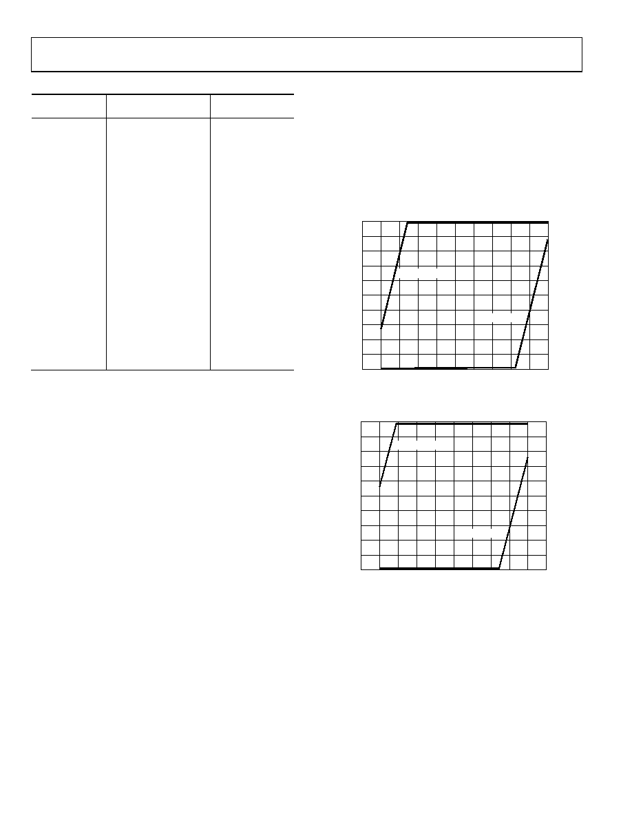
tends to decrease the voltage on A1. Figure 38 and Figure 39
show the maximum voltages that can be applied to the REF pin
for a gain of 5 for both the single-supply and dual-supply cases.
V
RE
F
(V)
VIN(–) (V)
5
–6
4
3
2
1
0
–1
–2
–3
–4
–5
–4
–3
–2
–1
0
1
2
3
4
MAXIMUM VREF
MINIMUM VREF
00782-
036
Figure 38. Reference Input Voltage vs. Negative Input Voltage,
VS = ±5 V, G = +5
V
RE
F
(V)
VIN(–) (V)
5
–0.5
4
3
2
1
0
0.5
1.0
2.0
1.5
2.5
3.0
3.5
4.0
4.5
MAXIMUM VREF
MINIMUM VREF
00782-
037
Figure 39. Reference Input Voltage vs. Negative Input Voltage,
VS = 5 V, G = +5
Raising the input common-mode voltage increases the voltage
on the output of A1. However, in single-supply applications
where the common-mode voltage is low, a differential input
voltage or a voltage on REF that is too high can drive the output
of A1 into the ground rail. Some low-side headroom is added
because both inputs are shifted upwards by about 0.5 V (that is,
by the VBE of Q1 and Q2). Use Equation 3 and Equation 4 to
check whether the voltage on Amplifier A1 is within its
operating range.
相关PDF资料 |
PDF描述 |
|---|---|
| KD1206PTB1 H.M. | FAN 12VDC 60X25.5MM 2.0W 22.5CFM |
| KD1208PTS3 H | FAN 12VDC 80X25MM 1.6W 31CFM |
| V511NA34 | VARISTR IND SQ DISC 510V 34MM NA |
| KD1208PTS2 H | FAN 12VDC 80X25MM 2.3W 36.5CFM |
| OP282GSZ | IC OPAMP JFET 4MHZ DUAL LP 8SOIC |
相关代理商/技术参数 |
参数描述 |
|---|---|
| AD627ARZ-RL | 功能描述:IC AMP INST R-R 25MA 8SOIC RoHS:是 类别:集成电路 (IC) >> Linear - Amplifiers - Instrumentation 系列:- 标准包装:2,500 系列:- 放大器类型:通用 电路数:2 输出类型:满摆幅 转换速率:350 V/µs 增益带宽积:180MHz -3db带宽:320MHz 电流 - 输入偏压:12.5µA 电压 - 输入偏移:800µV 电流 - 电源:15mA 电流 - 输出 / 通道:85mA 电压 - 电源,单路/双路(±):2.5 V ~ 12.6 V,±1.25 V ~ 6.3 V 工作温度:-40°C ~ 85°C 安装类型:表面贴装 封装/外壳:8-TSSOP,8-MSOP(0.118",3.00mm 宽) 供应商设备封装:8-MSOP 包装:带卷 (TR) |
| AD627B | 制造商:AD 制造商全称:Analog Devices 功能描述:Micropower, Single and Dual Supply Rail-to-Rail Instrumentation Amplifier |
| AD627BN | 制造商:Analog Devices 功能描述:SP Amp INSTR Amp Single R-R O/P ±18V/36V 8-Pin PDIP Tube 制造商:Rochester Electronics LLC 功能描述:PDIP UPOWER LOW COST INSTRUMENTATION AMP - Bulk |
| AD627BNZ | 功能描述:IC AMP INST R-R 25MA 8DIP RoHS:是 类别:集成电路 (IC) >> Linear - Amplifiers - Instrumentation 系列:- 标准包装:1 系列:- 放大器类型:通用 电路数:4 输出类型:满摆幅 转换速率:0.028 V/µs 增益带宽积:105kHz -3db带宽:- 电流 - 输入偏压:3nA 电压 - 输入偏移:100µV 电流 - 电源:3.3µA 电流 - 输出 / 通道:12mA 电压 - 电源,单路/双路(±):2.7 V ~ 12 V,±1.35 V ~ 6 V 工作温度:-40°C ~ 85°C 安装类型:表面贴装 封装/外壳:14-TSSOP(0.173",4.40mm 宽) 供应商设备封装:14-TSSOP 包装:剪切带 (CT) 其它名称:OP481GRUZ-REELCT |
| AD627BR | 功能描述:IC AMP INST R-R 25MA 8SOIC RoHS:否 类别:集成电路 (IC) >> Linear - Amplifiers - Instrumentation 系列:- 标准包装:50 系列:- 放大器类型:J-FET 电路数:2 输出类型:- 转换速率:3.5 V/µs 增益带宽积:1MHz -3db带宽:- 电流 - 输入偏压:30pA 电压 - 输入偏移:2000µV 电流 - 电源:200µA 电流 - 输出 / 通道:- 电压 - 电源,单路/双路(±):7 V ~ 36 V,±3.5 V ~ 18 V 工作温度:0°C ~ 70°C 安装类型:通孔 封装/外壳:8-DIP(0.300",7.62mm) 供应商设备封装:8-PDIP 包装:管件 |
发布紧急采购,3分钟左右您将得到回复。