参数资料
| 型号: | AD627BRZ |
| 厂商: | Analog Devices Inc |
| 文件页数: | 7/25页 |
| 文件大小: | 0K |
| 描述: | IC AMP INST R-R 25MA 8SOIC |
| 产品培训模块: | Power Line Monitoring Instrumentation Amplifiers Performance |
| 标准包装: | 98 |
| 放大器类型: | 仪表 |
| 电路数: | 1 |
| 输出类型: | 满摆幅 |
| 转换速率: | 0.06 V/µs |
| -3db带宽: | 80kHz |
| 电流 - 输入偏压: | 2nA |
| 电压 - 输入偏移: | 25µV |
| 电流 - 电源: | 60µA |
| 电流 - 输出 / 通道: | 25mA |
| 电压 - 电源,单路/双路(±): | 2.2 V ~ 36 V,±1.1 V ~ 18 V |
| 工作温度: | -40°C ~ 85°C |
| 安装类型: | 表面贴装 |
| 封装/外壳: | 8-SOIC(0.154",3.90mm 宽) |
| 供应商设备封装: | 8-SO |
| 包装: | 管件 |
| 产品目录页面: | 771 (CN2011-ZH PDF) |
AD627
Data Sheet
Rev. E | Page 14 of 24
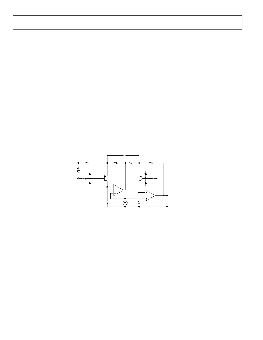
THEORY OF OPERATION
The AD627 is a true instrumentation amplifier, built using two
feedback loops. Its general properties are similar to those of the
classic two-op-amp instrumentation amplifier configuration but
internally the details are somewhat different. The AD627 uses a
modified current feedback scheme, which, coupled with interstage
feedforward frequency compensation, results in a much better
common-mode rejection ratio (CMRR) at frequencies above
dc (notably the line frequency of 50 Hz to 60 Hz) than might
otherwise be expected of a low power instrumentation amplifier.
In Figure 35, A1 completes a feedback loop that, in conjunction
with V1 and R5, forces a constant collector current in Q1. Assume
that the gain-setting resistor (RG) is not present. Resistors R2
and R1 complete the loop and force the output of A1 to be equal
to the voltage on the inverting terminal with a gain of nearly
1.25. A2 completes a nearly identical feedback loop that forces
a current in Q2 that is nearly identical to that in Q1; A2 also
provides the output voltage. When both loops are balanced, the
gain from the noninverting terminal to VOUT is equal to 5,
whereas the gain from the output of A1 to VOUT is equal to 4.
The inverting terminal gain of A1 (1.25) times the gain of A2
(4) makes the gain from the inverting and noninverting
terminals equal.
The differential mode gain is equal to 1 + R4/R3, nominally 5,
and is factory trimmed to 0.01% final accuracy. Adding an
external gain setting resistor (RG) increases the gain by an
amount equal to (R4 + R1)/RG. The output voltage of the
AD627 is given by
VOUT = [VIN(+) – VIN()] × (5 + 200 k/RG) + VREF
(1)
Laser trims are performed on R1 through R4 to ensure that
their values are as close as possible to the absolute values in the
gain equation. This ensures low gain error and high common-
mode rejection at all practical gains.
RG
EXTERNAL GAIN RESISTOR
REF
–IN
+IN
+VS
–VS
+VS
R1
100k
R2
25k
R5
200k
R6
200k
R3
25k
2k
0.1V
V1
A2
A1
Q1
Q2
OUTPUT
R4
100k
00782-
033
Figure 35. Simplified Schematic
相关PDF资料 |
PDF描述 |
|---|---|
| 929400-01-17 | CONN HEADER .100 SNGL STR 17POS |
| AD847JRZ | IC OPAMP GP 50MHZ LP 32MA 8SOIC |
| AD8513ARZ | IC OPAMP JFET 8MHZ QUAD 14SOIC |
| 929834-02-17 | CONN HEADER .100 SNGL STR 17POS |
| AD8513ARUZ | IC OPAMP JFET 8MHZ QUAD 14TSSOP |
相关代理商/技术参数 |
参数描述 |
|---|---|
| AD627BRZ-R7 | 功能描述:IC AMP INST R-R 80MHZ DL 8SOIC RoHS:是 类别:集成电路 (IC) >> Linear - Amplifiers - Instrumentation 系列:- 标准包装:2,500 系列:- 放大器类型:通用 电路数:4 输出类型:- 转换速率:0.6 V/µs 增益带宽积:1MHz -3db带宽:- 电流 - 输入偏压:45nA 电压 - 输入偏移:2000µV 电流 - 电源:1.4mA 电流 - 输出 / 通道:40mA 电压 - 电源,单路/双路(±):3 V ~ 32 V,±1.5 V ~ 16 V 工作温度:0°C ~ 70°C 安装类型:表面贴装 封装/外壳:14-TSSOP(0.173",4.40mm 宽) 供应商设备封装:14-TSSOP 包装:带卷 (TR) 其它名称:LM324ADTBR2G-NDLM324ADTBR2GOSTR |
| AD627BRZ-RL | 功能描述:IC AMP INST R-R 25MA 8SOIC RoHS:是 类别:集成电路 (IC) >> Linear - Amplifiers - Instrumentation 系列:- 标准包装:50 系列:- 放大器类型:J-FET 电路数:2 输出类型:- 转换速率:13 V/µs 增益带宽积:3MHz -3db带宽:- 电流 - 输入偏压:65pA 电压 - 输入偏移:3000µV 电流 - 电源:1.4mA 电流 - 输出 / 通道:- 电压 - 电源,单路/双路(±):7 V ~ 36 V,±3.5 V ~ 18 V 工作温度:-40°C ~ 85°C 安装类型:通孔 封装/外壳:8-DIP(0.300",7.62mm) 供应商设备封装:8-PDIP 包装:管件 |
| AD628 | 制造商:AD 制造商全称:Analog Devices 功能描述:Dual-Channel Audio Difference Amplifier |
| AD628_06 | 制造商:AD 制造商全称:Analog Devices 功能描述:High Common-Mode Voltage, Programmable Gain Difference Amplifier |
| AD628_07 | 制造商:AD 制造商全称:Analog Devices 功能描述:High Common-Mode Voltage, Programmable Gain Difference Amplifier |
发布紧急采购,3分钟左右您将得到回复。