参数资料
| 型号: | AD628ARZ-R7 |
| 厂商: | Analog Devices Inc |
| 文件页数: | 9/21页 |
| 文件大小: | 0K |
| 描述: | IC AMP PGA DIFF PREC 8SOIC |
| 标准包装: | 1,000 |
| 放大器类型: | 电流检测 |
| 电路数: | 1 |
| 转换速率: | 0.3 V/µs |
| -3db带宽: | 600kHz |
| 电流 - 输入偏压: | 1.5nA |
| 电压 - 输入偏移: | 150µV |
| 电流 - 电源: | 1.6mA |
| 电压 - 电源,单路/双路(±): | 4.5 V ~ 36 V,±2.25 V ~ 18 V |
| 工作温度: | -40°C ~ 85°C |
| 安装类型: | 表面贴装 |
| 封装/外壳: | 8-SOIC(0.154",3.90mm 宽) |
| 供应商设备封装: | 8-SO |
| 包装: | 带卷 (TR) |
AD628
Rev. G | Page 16 of 20
APPLICATIONS INFORMATION
GAIN ADJUSTMENT
The AD628 system gain is provided by an architecture
consisting of two amplifiers (see Figure 29). The gain of the
input stage is fixed at 0.1; the output buffer is user adjustable
as GA2 = 1 + REXT1/REXT2. The system gain is then
+
×
=
EXT2
EXT1
TOTAL
R
G
1
0.1
(1)
At a 2 nA maximum, the input bias current of the buffer amplifier
is very low and any offset voltage induced at the buffer amplifier
by its bias current may be neglected (2 nA × 10 kΩ = 20 μV).
However, to absolutely minimize bias current effects, select
REXT1 and REXT2 so that their parallel combination is 10 kΩ. If
practical resistor values force the parallel combination of REXT1
and REXT2 below 10 kΩ, add a series resistor (REXT3) to make up
for the difference. Table 5 lists several values of gain and
corresponding resistor values.
Table 5. Nearest Standard 1% Resistor Values for
Various Gains (see Figure 29)
Total Gain
(V/V)
A2 Gain
(V/V)
REXT1 (Ω)
REXT2 (Ω)
REXT3 (Ω)
0.1
1
10 k
∞
0
0.2
2
20 k
0
0.25
2.5
25.9 k
18.7 k
0
0.5
5
49.9 k
12.4 k
0
1
10
100 k
11 k
0
2
20
200 k
10.5 k
0
5
50
499 k
10.2 k
0
10
100
1 M
10.2 k
0
To set the system gain to <0.1, create an attenuator by placing
Resistor REXT4 from Pin 4 (CFILT) to the reference voltage. A
divider is formed by the 10 kΩ resistor that is in series with the
positive input of A2 and Resistor REXT4. A2 is configured for
unity gain.
Using a divider and setting A2 to unity gain yields
1
kΩ
10
0.1
/
×
+
×
=
EXT4
DIVIDER
W
R
G
INPUT VOLTAGE RANGE
VREF and the supply voltage determine the common-mode
input voltage range. The relation is expressed by
REF
S
CM
V
UPPER
10
)
V
2
.
1
–
(
11
≤
+
(2)
REF
S
CM
V
10
)
V
2
.
1
(
11
V
LOWER
+
≥
where:
VS+ is the positive supply.
VS is the negative supply.
1.2 V is the headroom needed for suitable performance.
Equation 2 provides a general formula for calculating the
common-mode input voltage range. However, keep the AD628
within the maximum limits listed in Table 1 to maintain
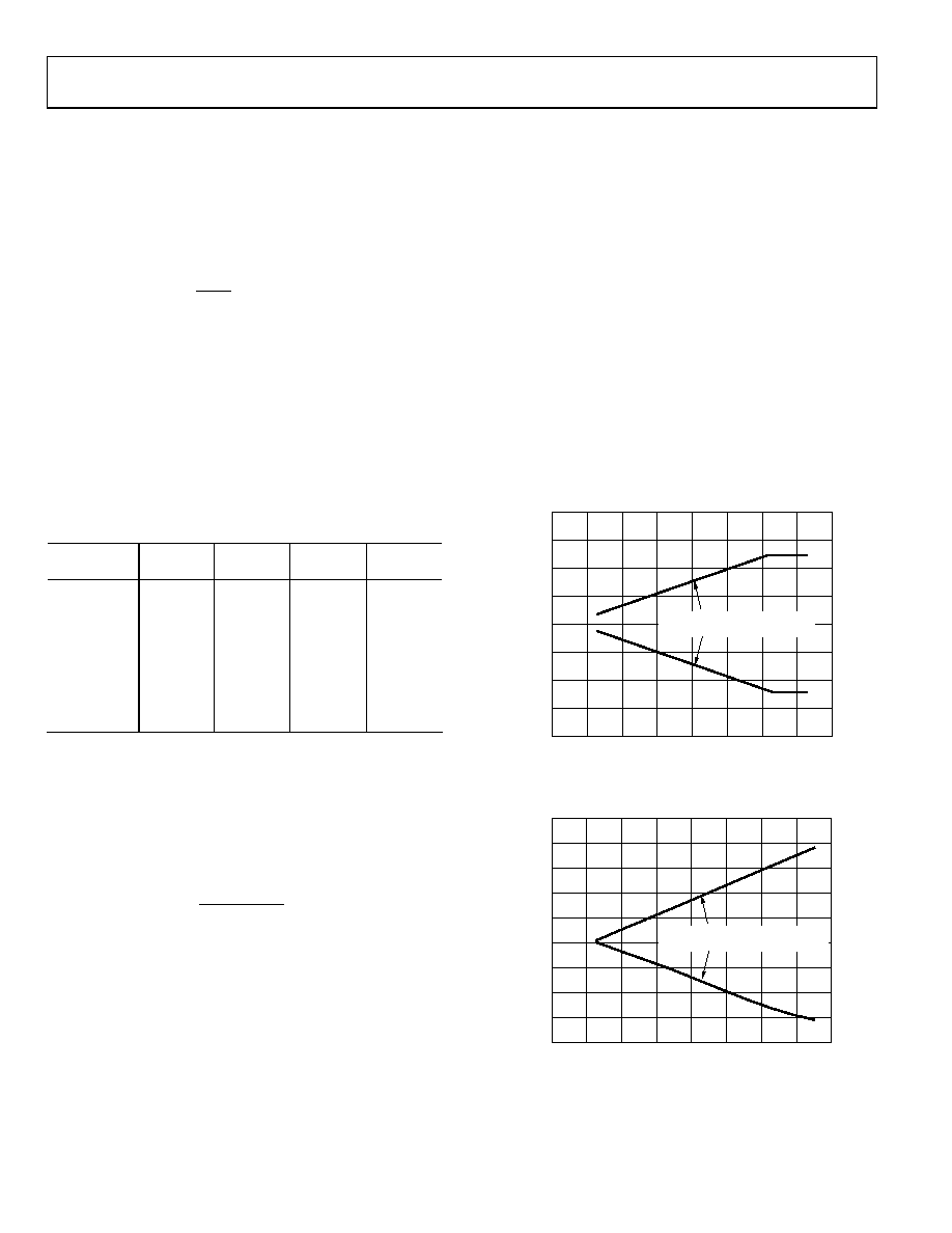
optimal performance. This is illustrated in Figure 30 where the
maximum common-mode input voltage is limited to ±120 V.
Figure 31 shows the common-mode input voltage bounds for
single-supply voltages.
–200
–150
–100
–50
0
50
IN
PU
T
C
O
MM
O
N
-M
O
D
E
VO
LT
A
G
E
(
V
)
100
150
200
8
6
24
010
12
SUPPLY VOLTAGE (±V)
02
99
2-
03
5
14
16
MAXIMUM INPUT COMMON-MODE
VOLTAGE WHEN VREF = GND
Figure 30. Input Common-Mode Voltage vs. Supply Voltage
for Dual Supplies
–80
–60
–40
–20
0
20
40
60
80
100
IN
PU
T
C
O
MM
O
N
-M
O
D
E
VO
LT
A
G
E
(
V
)
8
6
24
010
12
SINGLE-SUPPLY VOLTAGE (V)
02
99
2-
0
34
14
16
MAXIMUM INPUT COMMON-MODE
VOLTAGE WHEN VREF = MIDSUPPLY
Figure 31. Input Common-Mode Voltage vs.
Supply Voltage for Single Supplies
相关PDF资料 |
PDF描述 |
|---|---|
| 0001.2527 | FUSE 2A 250V 6.3X32 T-LAG |
| 0459858312 | CONN HEADER 8PWR 12SGL 2.36MM |
| AD628ARMZ-R7 | IC AMP PGA DIFF PREC 8MSOP |
| 0001.2529 | FUSE 3.15A 250V 6.3X32 T-LAG |
| 0702871033 | CONN HEADER BKWY DL TIN 70POS |
相关代理商/技术参数 |
参数描述 |
|---|---|
| AD628ARZ-RL | 功能描述:IC AMP PGA DIFF PREC 8SOIC RoHS:是 类别:集成电路 (IC) >> Linear - Amplifiers - Instrumentation 系列:- 标准包装:50 系列:- 放大器类型:通用 电路数:2 输出类型:满摆幅 转换速率:1.8 V/µs 增益带宽积:6.5MHz -3db带宽:4.5MHz 电流 - 输入偏压:5nA 电压 - 输入偏移:100µV 电流 - 电源:65µA 电流 - 输出 / 通道:35mA 电压 - 电源,单路/双路(±):1.8 V ~ 5.25 V,±0.9 V ~ 2.625 V 工作温度:-40°C ~ 85°C 安装类型:表面贴装 封装/外壳:10-TFSOP,10-MSOP(0.118",3.00mm 宽) 供应商设备封装:10-MSOP 包装:管件 |
| AD628-EVAL | 制造商:Analog Devices 功能描述:Evaluation Board For High Voltage Current Shunt Sensing |
| AD629 | 制造商:AD 制造商全称:Analog Devices 功能描述:Dual-Channel Audio Difference Amplifier |
| AD629_07 | 制造商:AD 制造商全称:Analog Devices 功能描述:High Common-Mode Voltage, Difference Amplifier |
| AD629A | 制造商:AD 制造商全称:Analog Devices 功能描述:High Common-Mode Voltage Difference Amplifier |
发布紧急采购,3分钟左右您将得到回复。