参数资料
| 型号: | AD629AN |
| 厂商: | Analog Devices Inc |
| 文件页数: | 4/16页 |
| 文件大小: | 0K |
| 描述: | IC AMP DIFF 25MA LDRIFT 8DIP |
| 产品变化通告: | Product Discontinuance 27/Oct/2011 |
| 设计资源: | Measuring -48 V High-Side Current Using AD629, AD8603, AD780, and AD7453 (CN0100) |
| 标准包装: | 50 |
| 放大器类型: | 差分 |
| 电路数: | 1 |
| 转换速率: | 2.1 V/µs |
| -3db带宽: | 500kHz |
| 电压 - 输入偏移: | 200µV |
| 电流 - 电源: | 900µA |
| 电流 - 输出 / 通道: | 25mA |
| 电压 - 电源,单路/双路(±): | 5 V ~ 36 V,±2.5 V ~ 18 V |
| 工作温度: | -40°C ~ 85°C |
| 安装类型: | 通孔 |
| 封装/外壳: | 8-DIP(0.300",7.62mm) |
| 供应商设备封装: | 8-PDIP |
| 包装: | 管件 |
AD629
Rev. C | Page 12 of 16
ANALOG POWER
SUPPLY
DIGITAL
POWER SUPPLY
0.1F
+IN
–IN
–VS
VIN1
VIN2
VDD
OUTPUT
AGND
GND
MICROPROCESSOR
DGND
+VS
AD629
AD7892-2
REF(–) REF(+)
6
7
14
4
1
3
2
6
4
1
5
12
+5V
GND
+5V
GND
–5V
007
83-
032
Figure 34. Optimal Grounding Practice for a Bipolar Supply Environment
with Separate Analog and Digital Supplies
POWER SUPPLY
VIN1
VIN2
VDD
AGND DGND
ADC
0.1F
+IN
–IN
+VS
OUTPUT
–VS
AD629
REF(–) REF(+)
4
7
3
2
6
1
5
VDD
GND
MICROPROCESSOR
+5V
GND
0.1F
00
783
-0
33
Figure 35. Optimal Ground Practice in a Single-Supply Environment
If there is only a single power supply available, it must be shared
by both digital and analog circuitry. Figure 35 shows how to
minimize interference between the digital and analog circuitry.
In this example, the ADC’s reference is used to drive Pin REF(+)
and Pin REF(–). This means that the reference must be capable
of sourcing and sinking a current equal to VCM/200 kΩ. As in
the previous case, separate analog and digital ground planes
should be used (reasonably thick traces can be used as an
alternative to a digital ground plane). These ground planes
should connect at the power supply’s ground pin. Separate
traces (or power planes) should run from the power supply to
the supply pins of the digital and analog circuits. Ideally, each
device should have its own power supply trace, but these can be
shared by a number of devices, as long as a single trace is not
used to route current to both digital and analog circuitry.
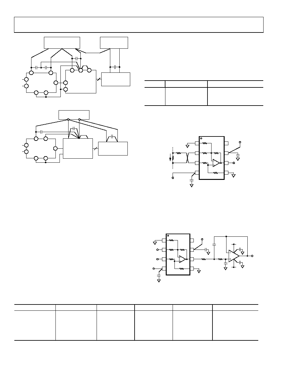
USING A LARGE SENSE RESISTOR
Insertion of a large value shunt resistance across the input pins,
Pin 2 and Pin 3, will imbalance the input resistor network,
introducing a common-mode error. The magnitude of the error
will depend on the common-mode voltage and the magnitude
of RSHUNT.
Table 5 shows some sample error voltages generated by a
common-mode voltage of 200 V dc with shunt resistors from
20 Ω to 2000 Ω. Assuming that the shunt resistor is selected to
use the full ±10 V output swing of the AD629, the error voltage
becomes quite significant as RSHUNT increases.
Table 5. Error Resulting from Large Values of RSHUNT
(Uncompensated Circuit)
RS (Ω)
Error VOUT (V)
Error Indicated (mA)
20
0.01
0.5
1000
0.498
2000
1
0.5
To measure low current or current near zero in a high common-
mode environment, an external resistor equal to the shunt
resistor value can be added to the low impedance side of the
shunt resistor, as shown in Figure 36.
REF (–)
REF (+)
–VS
+VS
VOUT
NC
–IN
+IN
RSHUNT
RCOMP
ISHUNT
0.1F
NC = NO CONNECT
21.1k
380k
20k
380k
AD629
1
2
3
4
8
7
6
5
00
78
3-
03
4
Figure 36. Compensating for Large Sense Resistors
OUTPUT FILTERING
A simple 2-pole, low-pass Butterworth filter can be implemented
using the OP177 after the AD629 to limit noise at the output, as
values for various corner frequencies, along with the peak-to-
peak output noise for each case.
REF (–)
REF (+)
–VS
+VS
VOUT
NC
–IN
+IN
0.1F
NC = NO CONNECT
21.1k
380k
20k
380k
AD629
1
2
3
4
8
7
6
5
00783
-035
R1
R2
C1
C2
OP177
Figure 37. Filtering of Output Noise Using a 2-Pole Butterworth Filter
Table 6. Recommended Values for 2-Pole Butterworth Filter
Corner Frequency
R1
R2
C1
C2
Output Noise (p-p)
No Filter
3.2 mV
50 kHz
2.94 kΩ ± 1%
1.58 kΩ ± 1%
2.2 nF ± 10%
1 nF ± 10%
1 mV
5 kHz
2.94 kΩ ± 1%
1.58 kΩ ± 1%
22 nF ± 10%
10 nF ± 10%
0.32 mV
500 Hz
2.94 kΩ ± 1%
1.58 kΩ ± 1%
220 nF ± 10%
0.1 μF ± 10%
100 μV
50 Hz
2.7 kΩ ± 10%
1.5 kΩ ± 10%
2.2 μF ± 20%
1 μF ± 20%
32 μV
相关PDF资料 |
PDF描述 |
|---|---|
| TSW-127-17-L-S | CONN HEADER 27POS .100" SGL GOLD |
| 8020.0519.PT | FUSE 3.15A 250VAC AXIAL SLOW |
| 8020.0518.PT | FUSE 2.5A 250VAC AXIAL SLOW |
| 8020.0517.PT | FUSE 2A 250VAC AXIAL SLOW |
| 8020.0516.PT | FUSE 1.6A 250VAC AXIAL SLOW |
相关代理商/技术参数 |
参数描述 |
|---|---|
| AD629ANZ | 功能描述:IC AMP DIFF 25MA LDRIFT 8DIP RoHS:是 类别:集成电路 (IC) >> Linear - Amplifiers - Instrumentation 系列:- 标准包装:2,500 系列:- 放大器类型:通用 电路数:4 输出类型:- 转换速率:0.6 V/µs 增益带宽积:1MHz -3db带宽:- 电流 - 输入偏压:45nA 电压 - 输入偏移:2000µV 电流 - 电源:1.4mA 电流 - 输出 / 通道:40mA 电压 - 电源,单路/双路(±):3 V ~ 32 V,±1.5 V ~ 16 V 工作温度:0°C ~ 70°C 安装类型:表面贴装 封装/外壳:14-TSSOP(0.173",4.40mm 宽) 供应商设备封装:14-TSSOP 包装:带卷 (TR) 其它名称:LM324ADTBR2G-NDLM324ADTBR2GOSTR |
| AD629ANZ | 制造商:Analog Devices 功能描述:IC AMP DIFF HI COM MODE VOLT ((SP)) |
| AD629AR | 功能描述:IC AMP DIFF 25MA LDRIFT 8SOIC RoHS:否 类别:集成电路 (IC) >> Linear - Amplifiers - Instrumentation 系列:- 标准包装:150 系列:- 放大器类型:音频 电路数:2 输出类型:- 转换速率:5 V/µs 增益带宽积:12MHz -3db带宽:- 电流 - 输入偏压:100nA 电压 - 输入偏移:500µV 电流 - 电源:6mA 电流 - 输出 / 通道:50mA 电压 - 电源,单路/双路(±):4 V ~ 32 V,±2 V ~ 16 V 工作温度:-40°C ~ 85°C 安装类型:表面贴装 封装/外壳:8-TSSOP(0.173",4.40mm 宽) 供应商设备封装:8-TSSOP 包装:管件 |
| AD629AR-REEL | 功能描述:IC AMP DIFF 25MA LDRIFT 8SOIC RoHS:否 类别:集成电路 (IC) >> Linear - Amplifiers - Instrumentation 系列:- 标准包装:73 系列:Over-The-Top® 放大器类型:通用 电路数:4 输出类型:满摆幅 转换速率:0.07 V/µs 增益带宽积:200kHz -3db带宽:- 电流 - 输入偏压:1nA 电压 - 输入偏移:285µV 电流 - 电源:50µA 电流 - 输出 / 通道:25mA 电压 - 电源,单路/双路(±):2 V ~ 44 V,±1 V ~ 22 V 工作温度:-40°C ~ 85°C 安装类型:表面贴装 封装/外壳:16-WFDFN 裸露焊盘 供应商设备封装:16-DFN-EP(5x3) 包装:管件 |
| AD629AR-REEL7 | 功能描述:IC AMP DIFF 25MA LDRIFT 8SOIC RoHS:否 类别:集成电路 (IC) >> Linear - Amplifiers - Instrumentation 系列:- 标准包装:73 系列:Over-The-Top® 放大器类型:通用 电路数:4 输出类型:满摆幅 转换速率:0.07 V/µs 增益带宽积:200kHz -3db带宽:- 电流 - 输入偏压:1nA 电压 - 输入偏移:285µV 电流 - 电源:50µA 电流 - 输出 / 通道:25mA 电压 - 电源,单路/双路(±):2 V ~ 44 V,±1 V ~ 22 V 工作温度:-40°C ~ 85°C 安装类型:表面贴装 封装/外壳:16-WFDFN 裸露焊盘 供应商设备封装:16-DFN-EP(5x3) 包装:管件 |
发布紧急采购,3分钟左右您将得到回复。