参数资料
| 型号: | AD629BR |
| 厂商: | Analog Devices Inc |
| 文件页数: | 3/16页 |
| 文件大小: | 0K |
| 描述: | IC AMP DIFF 25MA LDRIFT 8SOIC |
| 设计资源: | Measuring -48 V High-Side Current Using AD629, AD8603, AD780, and AD7453 (CN0100) |
| 标准包装: | 1 |
| 放大器类型: | 差分 |
| 电路数: | 1 |
| 转换速率: | 2.1 V/µs |
| -3db带宽: | 500kHz |
| 电压 - 输入偏移: | 100µV |
| 电流 - 电源: | 900µA |
| 电流 - 输出 / 通道: | 25mA |
| 电压 - 电源,单路/双路(±): | 5 V ~ 36 V,±2.5 V ~ 18 V |
| 工作温度: | -40°C ~ 85°C |
| 安装类型: | 表面贴装 |
| 封装/外壳: | 8-SOIC(0.154",3.90mm 宽) |
| 供应商设备封装: | 8-SO |
| 包装: | 管件 |
AD629
Rev. C | Page 11 of 16
APPLICATIONS
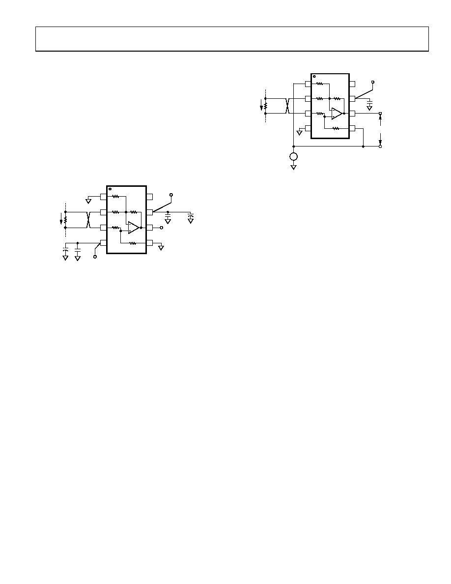
BASIC CONNECTIONS
Figure 32 shows the basic connections for operating the AD629
with a dual supply. A supply voltage of between ±3 V and ±18 V
is applied between Pin 7 and Pin 4. Both supplies should be
decoupled close to the pins using 0.1 μF capacitors. Electrolytic
capacitors of 10 μF, also located close to the supply pins, may be
required if low frequency noise is present on the power supply.
While multiple amplifiers can be decoupled by a single set of
10 μF capacitors, each in amp should have its own set of 0.1 μF
capacitors so that the decoupling point can be located right at
the IC’s power pins.
REF (–)
REF (+)
–VS
+VS
VOUT = ISHUNT × RSHUNT
NC
–IN
+IN
RSHUNT
ISHUNT
(SEE
TEXT)
(SEE
TEXT)
0.1F
+3V TO +18V
–3V TO –18V
NC = NO CONNECT
21.1k
380k
20k
380k
AD629
1
2
3
4
8
7
6
5
00
78
3-
0
3
0
Figure 32. Basic Connections
The differential input signal, which typically results from a load
current flowing through a small shunt resistor, is applied to
Pin 2 and Pin 3 with the polarity shown to obtain a positive
gain. The common-mode range on the differential input signal
can range from 270 V to +270 V, and the maximum differential
range is ±13 V. When configured as shown in Figure 32, the
device operates as a simple gain-of-1, differential-to-single-
ended amplifier; the output voltage being the shunt resistance
times the shunt current. The output is measured with respect to
Pin 1 and Pin 5.
Pin 1 and Pin 5 (REF(–) and REF(+)) should be grounded for a
gain of unity and should be connected to the same low impedance
ground plane. Failure to do this results in degraded common-
mode rejection. Pin 8 is a no connect pin and should be left open.
SINGLE-SUPPLY OPERATION
Figure 33 shows the connections for operating the AD629 with
a single supply. Because the output can swing to within only
about 2 V of either rail, it is necessary to apply an offset to the
output. This can be conveniently done by connecting REF(+)
and REF(–) to a low impedance reference voltage (some ADCs
provide this voltage as an output), which is capable of sinking
current. Therefore, for a single supply of 10 V, VREF may be set
to 5 V for a bipolar input signal. This allows the output to swing
±3 V around the central 5 V reference voltage. Alternatively, for
unipolar input signals, VREF can be set to about 2 V, allowing the
output to swing from 2 V (for a 0 V input) to within 2 V of the
positive rail.
REF (–)
REF (+)
–VS
VY
VX
+VS
NC
–IN
+IN
RSHUNT
ISHUNT
0.1F
NC = NO CONNECT
21.1k
380k
20k
380k
AD629
1
2
3
4
8
7
6
5
00783-
031
OUTPUT = VOUT – VREF
VREF
Figure 33. Operation with a Single Supply
Applying a reference voltage to REF(+) and REF(–) and
operating on a single supply reduces the input common-mode
range of the AD629. The new input common-mode range
depends upon the voltage at the inverting and noninverting
inputs of the internal operational amplifier, labeled VX and VY
in Figure 33. These nodes can swing to within 1 V of either rail.
Therefore, for a (single) supply voltage of 10 V, VX and VY can
range between 1 V and 9 V. If VREF is set to 5 V, the permissible
common-mode range is +85 V to –75 V. The common-mode
voltage ranges can be calculated by
VCM (±) = 20 VX/VY(±) 19 VREF
SYSTEM-LEVEL DECOUPLING AND GROUNDING
The use of ground planes is recommended to minimize the
impedance of ground returns (and therefore the size of dc
errors). Figure 34 shows how to work with grounding in a
mixed-signal environment, that is, with digital and analog
signals present. To isolate low level analog signals from a noisy
digital environment, many data acquisition components have
separate analog and digital ground returns. All ground pins
from mixed-signal components, such as ADCs, should return
through a low impedance analog ground plane. Digital ground
lines of mixed-signal converters should also be connected to the
analog ground plane. Typically, analog and digital grounds
should be separated; however, it is also a requirement to
minimize the voltage difference between digital and analog
grounds on a converter, to keep them as small as possible
(typically <0.3 V). The increased noise, caused by the
converter’s digital return currents flowing through the analog
ground plane, is typically negligible. Maximum isolation
between analog and digital is achieved by connecting the ground
planes back at the supplies. Note that Figure 34 suggests a “star”
ground system for the analog circuitry, with all ground lines
being connected, in this case, to the ADC’s analog ground.
However, when ground planes are used, it is sufficient to
connect ground pins to the nearest point on the low impedance
ground plane.
相关PDF资料 |
PDF描述 |
|---|---|
| 1-521253-2 | CONN RCPT HSG 2POS .250 RED |
| AD9632AR | IC OPAMP VF ULDIST 70MA 8SOIC |
| LT2179IS#TRPBF | IC OPAMP MICROPOWER QUAD 14SOIC |
| RNCP0805FTD8K25 | RES 8.25K OHM 1/4W 1% 0805 SMD |
| AD8036AN | IC OPAMP VF ULDIST LN 70MA 8DIP |
相关代理商/技术参数 |
参数描述 |
|---|---|
| AD629BR-REEL | 功能描述:IC AMP DIFF 25MA LDRIFT 8SOIC RoHS:否 类别:集成电路 (IC) >> Linear - Amplifiers - Instrumentation 系列:- 标准包装:150 系列:- 放大器类型:音频 电路数:2 输出类型:- 转换速率:5 V/µs 增益带宽积:12MHz -3db带宽:- 电流 - 输入偏压:100nA 电压 - 输入偏移:500µV 电流 - 电源:6mA 电流 - 输出 / 通道:50mA 电压 - 电源,单路/双路(±):4 V ~ 32 V,±2 V ~ 16 V 工作温度:-40°C ~ 85°C 安装类型:表面贴装 封装/外壳:8-TSSOP(0.173",4.40mm 宽) 供应商设备封装:8-TSSOP 包装:管件 |
| AD629BR-REEL7 | 功能描述:IC AMP DIFF 25MA LDRIFT 8SOIC RoHS:否 类别:集成电路 (IC) >> Linear - Amplifiers - Instrumentation 系列:- 标准包装:150 系列:- 放大器类型:音频 电路数:2 输出类型:- 转换速率:5 V/µs 增益带宽积:12MHz -3db带宽:- 电流 - 输入偏压:100nA 电压 - 输入偏移:500µV 电流 - 电源:6mA 电流 - 输出 / 通道:50mA 电压 - 电源,单路/双路(±):4 V ~ 32 V,±2 V ~ 16 V 工作温度:-40°C ~ 85°C 安装类型:表面贴装 封装/外壳:8-TSSOP(0.173",4.40mm 宽) 供应商设备封装:8-TSSOP 包装:管件 |
| AD629BRZ | 功能描述:IC AMP DIFF 25MA LDRIFT 8SOIC RoHS:是 类别:集成电路 (IC) >> Linear - Amplifiers - Instrumentation 系列:- 标准包装:2,500 系列:- 放大器类型:通用 电路数:4 输出类型:- 转换速率:0.6 V/µs 增益带宽积:1MHz -3db带宽:- 电流 - 输入偏压:45nA 电压 - 输入偏移:2000µV 电流 - 电源:1.4mA 电流 - 输出 / 通道:40mA 电压 - 电源,单路/双路(±):3 V ~ 32 V,±1.5 V ~ 16 V 工作温度:0°C ~ 70°C 安装类型:表面贴装 封装/外壳:14-TSSOP(0.173",4.40mm 宽) 供应商设备封装:14-TSSOP 包装:带卷 (TR) 其它名称:LM324ADTBR2G-NDLM324ADTBR2GOSTR |
| AD629BRZ-R7 | 功能描述:IC AMP DIFF 25MA LDRIFT 8SOIC RoHS:是 类别:集成电路 (IC) >> Linear - Amplifiers - Instrumentation 系列:- 标准包装:150 系列:- 放大器类型:音频 电路数:2 输出类型:- 转换速率:5 V/µs 增益带宽积:12MHz -3db带宽:- 电流 - 输入偏压:100nA 电压 - 输入偏移:500µV 电流 - 电源:6mA 电流 - 输出 / 通道:50mA 电压 - 电源,单路/双路(±):4 V ~ 32 V,±2 V ~ 16 V 工作温度:-40°C ~ 85°C 安装类型:表面贴装 封装/外壳:8-TSSOP(0.173",4.40mm 宽) 供应商设备封装:8-TSSOP 包装:管件 |
| AD629BRZ-RL | 功能描述:IC AMP DIFF 25MA LDRIFT 8SOIC RoHS:是 类别:集成电路 (IC) >> Linear - Amplifiers - Instrumentation 系列:- 标准包装:150 系列:- 放大器类型:音频 电路数:2 输出类型:- 转换速率:5 V/µs 增益带宽积:12MHz -3db带宽:- 电流 - 输入偏压:100nA 电压 - 输入偏移:500µV 电流 - 电源:6mA 电流 - 输出 / 通道:50mA 电压 - 电源,单路/双路(±):4 V ~ 32 V,±2 V ~ 16 V 工作温度:-40°C ~ 85°C 安装类型:表面贴装 封装/外壳:8-TSSOP(0.173",4.40mm 宽) 供应商设备封装:8-TSSOP 包装:管件 |
发布紧急采购,3分钟左右您将得到回复。