参数资料
| 型号: | AD640BP |
| 厂商: | Analog Devices Inc |
| 文件页数: | 15/16页 |
| 文件大小: | 0K |
| 描述: | IC AMP LOG 2.3MA 20PLCC |
| 标准包装: | 1 |
| 放大器类型: | 对数 |
| 电路数: | 1 |
| -3db带宽: | 350MHz |
| 电流 - 输入偏压: | 7µA |
| 电压 - 输入偏移: | 50µV |
| 电流 - 电源: | 35mA |
| 电流 - 输出 / 通道: | 2.3mA |
| 电压 - 电源,单路/双路(±): | ±4.5 V ~ 7.5 V |
| 工作温度: | -40°C ~ 85°C |
| 安装类型: | 表面贴装 |
| 封装/外壳: | 20-LCC(J 形引线) |
| 供应商设备封装: | 20-PLCC(9x9) |
| 包装: | 管件 |
AD640
REV. C
–8–
50
A/dB, or 1 mA per decade. This scaling parameter is
trimmed to absolute accuracy using a 2 kHz square wave. At
frequencies near the system bandwidth, the slope is reduced due
to the reduced output of the limiter stages, but it is still rela-
tively insensitive to temperature variations so that a simple ex-
ternal slope adjustment in restore scaling accuracy.
The intercept position bias generator (Figure 17) removes the
pedestal current from the summed detector outputs. It is ad-
justed during manufacture such that the output (flowing into
Pin 14) is 1 mA when a 2 kHz square-wave input of exactly
±10 mV is applied to the AD640. This places the dc intercept at
precisely 1 mV. The LOG COM output (Pin 13) is the comple-
ment of LOG OUT. It also has a 1 mV intercept, but with an
inverted slope of –1 mA/decade. Because its pedestal is very
large (equivalent to about 100 dB), its intercept voltage is not
guaranteed. The intercept positioning currents include a special
internal temperature compensation (ITC) term which can be
disabled by connecting Pin 8 to ground.
The logarithmic function of the AD640 is absolutely calibrated
to within
±0.3 dB (or ±15 A) for 2 kHz square-wave inputs of
±1 mV to ±100 mV, and to within ±1 dB between ±750 V and
±200 mV. Figure 18 is a typical plot of the dc transfer function,
showing the outputs at temperatures of –55
°C, +25°C and
+125
°C. While the slope and intercept are seen to be little af-
fected by temperature, there is a lateral shift in the endpoints of
the “linear” region of the transfer function, which reduces the
effective dynamic range. The cause of this shift is explained in
Fundamentals of Logarithmic Conversion section.
INPUT VOLTAGE – mV
2.5
0
0.1
OUTPUT
CURRENT
–
mA
1.0
10.0
100.0
1000.0
2
1
0
–1
–2
2.0
1.5
1.0
0.5
–0.5
+125 C
+25 C
–55 C
+25 C
+125 C
–55 C
ABSOLUTE
ERROR
–
dB
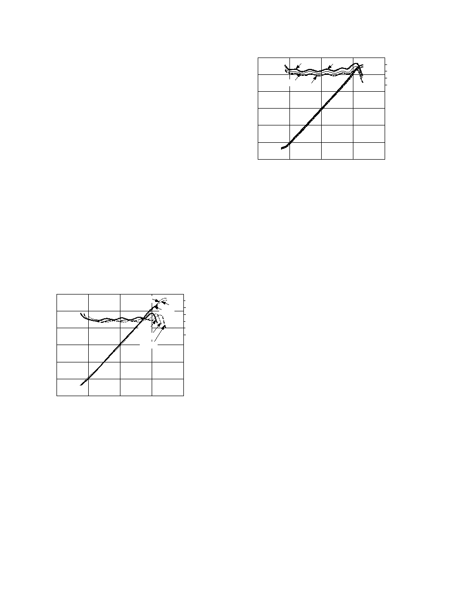
Figure 18. Logarithmic Output and Absolute Error vs. DC
or Square Wave Input at TA = –55°C, +25 °C, Input Direct
to Pins 1 and 20
The on chip attenuator can be used to handle input levels 20 dB
higher, that is, from
±7.5 mV to ±2 V for dc or square wave
inputs. It is specially designed to have a positive temperature
coefficient and is trimmed to position the intercept at 10 mV dc
(or –24 dBm for a sinusoidal input) over the full temperature
range. When using the attenuator the internal bias compensa-
tion should be disabled by grounding Pin 8. Figure 19 shows
the output at –55
°C, +25°C, +85°C and +125°C for a single
AD640 with the attenuator in use; the curves overlap almost
perfectly, and the lateral shift in the transfer function does not
occur. Therefore, the full dynamic range is available at all
temperatures.
The output of the final limiter is available in differential form at
Pins 10 and 11. The output impedance is 75
to ground from
either pin. For most input levels, this output will appear to have
INPUT VOLTAGE – mV
2.5
0
1
OUTPUT
CURRENT
–
mA
10
100
1000
10000
1
0
–1
–2
2.0
1.5
1.0
0.5
–0.5
+25 C
+85 C
+125 C
–55 C
ABSOLUTE
ERROR
–
dB
Figure 19. Logarithmic Output and Absolute Error vs. DC
or Square Wave Input at TA = –55°C, +25°C, +85 °C and
+125
°C, Input via On-Chip Attenuator
roughly a square waveform. The signal path may be extended
using these outputs (see OPERATION OF CASCADED
AD640s). The logarithmic outputs from two or more AD640s
can be directly summed with full accuracy.
A pair of 1 k
applications resistors, RG1 and RG2 (Figure 17)
are accessed via Pins 15, 16 and 17. These can be used to con-
vert an output current to a voltage, with a slope of 1 V/decade
(using one resistor), 2 V/decade (both resistors in series) or
0.5 V/decade (both in parallel). Using all the resistors from two
AD640s (for example, in a cascaded configuration) ten slope
options from 0.25 V to 4 V/decade are available.
FUNDAMENTALS OF LOGARITHMIC CONVERSION
The conversion of a signal to its equivalent logarithmic value
involves a nonlinear operation, the consequences of which can be
very confusing if not fully understood. It is important to realize
from the outset that many of the familiar concepts of linear
circuits are of little relevance in this context. For example, the
incremental gain of an ideal logarithmic converter approaches
infinity as the input approaches zero. Further, an offset at the
output of a linear amplifier is simply equivalent to an offset at
the input, while in a logarithmic converter it is equivalent to a
change of amplitude at the input—a very different relationship.
We assume a dc signal in the following discussion to simplify the
concepts; ac behavior and the effect of input waveform on cali-
bration are discussed later. A logarithmic converter having a
voltage input VIN and output VOUT must satisfy a transfer func-
tion of the form
VOUT = VY LOG (VIN/VX)
Equation (1)
where Vy and Vx are fixed voltages which determine the scaling
of the converter. The input is divided by a voltage because the
argument of a logarithm has to be a simple ratio. The logarithm
must be multiplied by a voltage to develop a voltage output.
These operations are not, of course, carried out by explicit com-
putational elements, but are inherent in the behavior of the
converter. For stable operation, VX and VY must be based on
sound design criteria and rendered stable over wide temperature
and supply voltage extremes. This aspect of RF logarithmic
amplifier design has traditionally received little attention.
When VIN = VX, the logarithm is zero. VX is, therefore, called
the Intercept Voltage, because a graph of VOUT versus LOG (VIN)
—ideally a straight line—crosses the horizontal axis at this point
相关PDF资料 |
PDF描述 |
|---|---|
| NTPA74R0LB4A0 | CURRENT LIMITER |
| NTPA74R0LB1A0 | CURRENT LIMITER |
| NTPA7220LB1A0 | CURRENT LIMITER |
| 77311-102T16LF | BERGSTIK |
| 77315-813-15LF | CONN HEADER .100 1ROW R/A 15POS |
相关代理商/技术参数 |
参数描述 |
|---|---|
| AD640BPZ | 功能描述:IC AMP LOG 2.3MA 20PLCC RoHS:是 类别:集成电路 (IC) >> Linear - Amplifiers - Instrumentation 系列:- 标准包装:1 系列:- 放大器类型:通用 电路数:4 输出类型:满摆幅 转换速率:0.028 V/µs 增益带宽积:105kHz -3db带宽:- 电流 - 输入偏压:3nA 电压 - 输入偏移:100µV 电流 - 电源:3.3µA 电流 - 输出 / 通道:12mA 电压 - 电源,单路/双路(±):2.7 V ~ 12 V,±1.35 V ~ 6 V 工作温度:-40°C ~ 85°C 安装类型:表面贴装 封装/外壳:14-TSSOP(0.173",4.40mm 宽) 供应商设备封装:14-TSSOP 包装:剪切带 (CT) 其它名称:OP481GRUZ-REELCT |
| AD640EB | 制造商:AD 制造商全称:Analog Devices 功能描述:DC-Coupled Demodulating 120 MHz Logarithmic Amplifier |
| AD640-EB | 制造商:Analog Devices 功能描述: |
| AD640J | 制造商:AD 制造商全称:Analog Devices 功能描述:DC-Coupled Demodulating 120 MHz Logarithmic Amplifier |
| AD640JN | 功能描述:IC AMP LOG 2.3MA 20DIP RoHS:否 类别:集成电路 (IC) >> Linear - Amplifiers - Instrumentation 系列:- 其它有关文件:TS1854A View All Specifications 标准包装:50 系列:- 放大器类型:通用 电路数:4 输出类型:满摆幅 转换速率:0.25 V/µs 增益带宽积:630kHz -3db带宽:- 电流 - 输入偏压:16nA 电压 - 输入偏移:1000µV 电流 - 电源:162µA 电流 - 输出 / 通道:48mA 电压 - 电源,单路/双路(±):1.8 V ~ 6 V 工作温度:-40°C ~ 125°C 安装类型:表面贴装 封装/外壳:14-SOIC(0.154",3.90mm 宽) 供应商设备封装:14-SO 包装:管件 |
发布紧急采购,3分钟左右您将得到回复。