参数资料
| 型号: | AD640BPZ |
| 厂商: | Analog Devices Inc |
| 文件页数: | 3/16页 |
| 文件大小: | 0K |
| 描述: | IC AMP LOG 2.3MA 20PLCC |
| 标准包装: | 1 |
| 放大器类型: | 对数 |
| 电路数: | 1 |
| -3db带宽: | 350MHz |
| 电流 - 输入偏压: | 7µA |
| 电压 - 输入偏移: | 50µV |
| 电流 - 电源: | 35mA |
| 电流 - 输出 / 通道: | 2.3mA |
| 电压 - 电源,单路/双路(±): | ±4.5 V ~ 7.5 V |
| 工作温度: | -40°C ~ 85°C |
| 安装类型: | 表面贴装 |
| 封装/外壳: | 20-LCC(J 形引线) |
| 供应商设备封装: | 20-PLCC(9x9) |
| 包装: | 管件 |
AD640
REV. C
–11–
IOUT = 50
A (Input
dBV + 60)
Equation (5)
Alternatively, for a sinusoidal input measured in dBm (power in
dB above 1 mW in a 50
system) the output can be written
IOUT = 50
A (Input
dBm + 44)
Equation (6)
because the intercept for a sine wave expressed in volts rms is at
1.414 mV (from Table I) or –44 dBm.
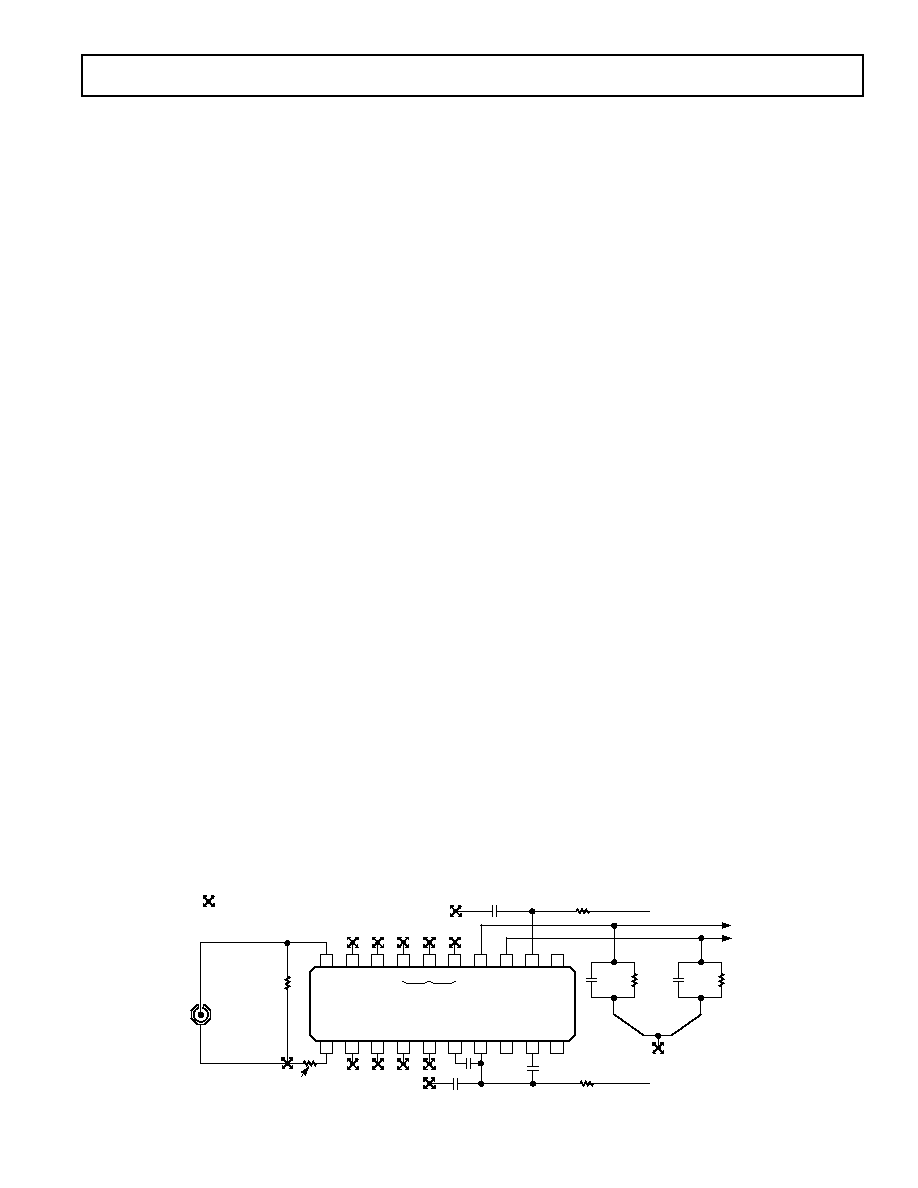
OPERATION OF A SINGLE AD640
Figure 24 shows the basic connections for a single device, using
100
load resistors. Output A is a negative going voltage with a
slope of –100 mV per decade; output B is positive going with a
slope of +100 mV per decade. For applications where absolute
calibration of the intercept is essential, the main output (from
LOG OUT, Pin 14) should be used; the LOG COM output can
then be grounded. To evaluate the demodulation response, a
simple low-pass output filter having a time constant of roughly
500
s (3 dB corner of 320 Hz) is provided by a 4.7 F (–20%
+80%) ceramic capacitor (Erie type RPE117-Z5U-475-K50V)
placed across the load. A DVM may be used to measure the
averaged output in verification tests. The voltage compliance at
Pins 13 and 14 extends from 0.3 V below ground up to 1 V
below +VS. Since the current into Pin 14 is from –0.2 mA at
zero signal to +2.3 mA when fully limited (dc input of >300 mV)
the output never drops below –230 mV. On the other hand, the
current out of Pin 13 ranges from 0.2 mA to +2.3 mA, and if
desired, a load resistor of up to 2 k
can be used on this output;
the slope would then be 2 V per decade. Use of the LOG COM
output in this way provides a numerically correct decibel read-
ing on a DVM (+100 mV = +1.00 dB).
Board layout is very important. The AD640 has both high gain
and wide bandwidth; therefore every signal path must be very
carefully considered. A high quality ground plane is essential,
but it should not be assumed that it behaves as an equipotential
plane. Even though the application may only call for modest
bandwidth, each of the three differential signal interface pairs
(SIG IN, Pins 1 and 20, SIG OUT, Pins 10 and 11, and LOG,
Pins 13 and 14) must have their own “starred” ground points to
avoid oscillation at low signal levels (where the gain is highest).
Unused pins (excluding Pins 8, 10 and 11) such as the attenua-
tor and applications resistors should be grounded close to the
package edge. BL1 (Pin 6) and BL2 (Pin 9) are internal bias
lines a volt or two above the –VS node; access is provided solely
for the addition of decoupling capacitors, which should be con-
nected exactly as shown (not all of them connect to the ground).
Use low impedance ceramic 0.1
F capacitors (for example,
Erie RPE113-Z5U-105-K50V). Ferrite beads may be used
instead of supply decoupling resistors in cases where the supply
voltage is low.
Active Current-to-Voltage Conversion
The compliance at LOG OUT limits the available output volt-
age swing. The output of the AD640 may be converted to a
larger, buffered output voltage by the addition of an operational
amplifier connected as a current-to-voltage (transresistance)
stage, as shown in Figure 21. Using a 2 k
feedback resistor
(R2) the 50
A/dB output at LOG OUT is converted to a volt-
age having a slope of +100 mV/dB, that is, 2 V per decade. This
output ranges from roughly –0.4 V for zero signal inputs to the
AD640, crosses zero at a dc input of precisely +1 mV (or
–1 mV) and is +4 V for a dc input of 100 mV. A passive
prefilter, formed by R1 and C1, minimizes the high frequency
energy conveyed to the op amp. The corner frequency is here
shown as 10 MHz. The AD844 is recommended for this appli-
cation because of its excellent performance in transresistance
modes. Its bandwidth of 35 MHz (with the 2 k
feedback resis-
tor) will exceed the baseband response of the system in most
applications. For lower bandwidth applications other op amps
and multipole active filters may be substituted (see, for example,
Figure 32 in the APPLICATIONS section).
Effect of Frequency on Calibration
The slope and intercept of the AD640 are calibrated during
manufacture using a 2 kHz square wave input. Calibration de-
pends on the gain of each stage being 10 dB. When the input
frequency is an appreciable fraction of the 350 MHz bandwidth
of the amplifier stages, their gain becomes imprecise and the
logarithmic slope and intercept are no longer fully calibrated.
However, the AD640 can provide very stable operation at fre-
quencies up to about one half the 3 dB frequency of the ampli-
fier stages. Figure 10 shows the averaged output current versus
input level at 30 MHz, 60 MHz, 90 MHz and 120 MHz. Fig-
ure 11 shows the absolute error in the response at 60 MHz and
at temperatures of –55
°C, +25°C and +125°C. Figure 12 shows
the variation in the slope current, and Figure 13 shows the
variation in the intercept level (sinusoidal input) versus frequency.
If absolute calibration is essential, or some other value of slope
or intercept is required, there will usually be some point in the
user’s system at which an adjustment may be easily introduced.
For example, the 5% slope deficit at 30 MHz (see Figure 12)
may be restored by a 5% increase in the value of the load resis-
tor in the passive loading scheme shown in Figure 24, or by
inserting a trim potentiometer of 100
in series with the feed-
back resistor in the scheme shown in Figure 21. The intercept
NC
RLA
100
0.1%
4.7 F
RLB
100
0.1%
4.7 F
OUTPUT A
OUTPUT B
NC
15
13
14
16
19
18
17
11
12
20
6
8
7
5
3
4
10
9
1
2
SIG
+IN
ATN
OUT
CKT
COM
RG1 RG0 RG2 LOG
OUT
LOG
COM
+VS
SIG
+OUT
SIG
–IN
ATN
LO
ATN
COM
BL1
BL2
ITC
–VS
SIG
–OUT
1k
ATN
COM
ATN
IN
AD640
NC
4.7
10
+5V
–5V
OPTIONAL
TERMINATION
RESISTOR
SIGNAL
INPUT
DENOTES A SHORT, DIRECT CONNECTION
TO THE GROUND PLANE.
ALL UNMARKED CAPACITORS ARE
0.1 F CERAMIC (SEE TEXT)
OPTIONAL
OFFSET BALANCE
RESISTOR
NC = NO CONNECT
Figure 24. Connections for a Single AD640 to Verify Basic Performance
相关PDF资料 |
PDF描述 |
|---|---|
| 4-103783-0-36 | CONN HEADR BRKWAY .100 72POS STR |
| AD684JQ | IC AMP SAMPLE HOLD QUAD 16CDIP |
| AD202KN | IC AMP ISOL 2KHZ DUAL LP 38DIP |
| AD625CDZ | IC AMP INST 25MHZ LN 16CDIP |
| 929647-04-29-I | CONN HEADER .100 SNGL STR 29POS |
相关代理商/技术参数 |
参数描述 |
|---|---|
| AD640EB | 制造商:AD 制造商全称:Analog Devices 功能描述:DC-Coupled Demodulating 120 MHz Logarithmic Amplifier |
| AD640-EB | 制造商:Analog Devices 功能描述: |
| AD640J | 制造商:AD 制造商全称:Analog Devices 功能描述:DC-Coupled Demodulating 120 MHz Logarithmic Amplifier |
| AD640JN | 功能描述:IC AMP LOG 2.3MA 20DIP RoHS:否 类别:集成电路 (IC) >> Linear - Amplifiers - Instrumentation 系列:- 其它有关文件:TS1854A View All Specifications 标准包装:50 系列:- 放大器类型:通用 电路数:4 输出类型:满摆幅 转换速率:0.25 V/µs 增益带宽积:630kHz -3db带宽:- 电流 - 输入偏压:16nA 电压 - 输入偏移:1000µV 电流 - 电源:162µA 电流 - 输出 / 通道:48mA 电压 - 电源,单路/双路(±):1.8 V ~ 6 V 工作温度:-40°C ~ 125°C 安装类型:表面贴装 封装/外壳:14-SOIC(0.154",3.90mm 宽) 供应商设备封装:14-SO 包装:管件 |
| AD640JN | 制造商:Analog Devices 功能描述:SEMICONDUCTORSLINEAR |
发布紧急采购,3分钟左右您将得到回复。