参数资料
| 型号: | AD640JPZ |
| 厂商: | Analog Devices Inc |
| 文件页数: | 1/16页 |
| 文件大小: | 0K |
| 描述: | IC AMP LOG 2.3MA 20PLCC |
| 标准包装: | 1 |
| 放大器类型: | 对数 |
| 电路数: | 1 |
| -3db带宽: | 350MHz |
| 电流 - 输入偏压: | 7µA |
| 电压 - 输入偏移: | 50µV |
| 电流 - 电源: | 35mA |
| 电流 - 输出 / 通道: | 2.3mA |
| 电压 - 电源,单路/双路(±): | ±4.5 V ~ 7.5 V |
| 工作温度: | 0°C ~ 70°C |
| 安装类型: | 表面贴装 |
| 封装/外壳: | 20-LCC(J 形引线) |
| 供应商设备封装: | 20-PLCC(9x9) |
| 包装: | 管件 |
ATN OUT
AMPLIFIER/LIMITER
FULL-WAVE
DETECTOR
ATN LO
ATN COM
SIG +IN
SIG –IN
ATN COM
COM
27
30
270
ATN IN
1k
RG1
RG0
RG2
–VS
BL1
+VS
LOG OUT
LOG COM
SIG +OUT
SIG –OUT
BL2
ITC
20
1
INTERCEPT POSITIONING BIAS
19
3
2
4
18
5
6
GAIN BIAS REGULATOR
AMPLIFIER/LIMITER
FULL-WAVE
DETECTOR
AMPLIFIER/LIMITER
FULL-WAVE
DETECTOR
10dB
AMPLIFIER/LIMITER
FULL-WAVE
DETECTOR
10dB
AMPLIFIER/LIMITER
FULL-WAVE
DETECTOR
17
16
14
13
1k
7
11
10
9
8
12
SLOPE BIAS REGULATOR
15
10dB
a
DC-Coupled Demodulating
120 MHz Logarithmic Amplifier
AD640
One Technology Way, P.O. Box 9106, Norwood, MA 02062-9106, U.S.A.
Tel: 781/329-4700
World Wide Web Site: http://www.analog.com
Fax: 781/326-8703
Analog Devices, Inc., 1999
FEATURES
Complete, Fully Calibrated Monolithic System
Five Stages, Each Having 10 dB Gain, 350 MHz BW
Direct Coupled Fully Differential Signal Path
Logarithmic Slope, Intercept and AC Response are
Stable Over Full Military Temperature Range
Dual Polarity Current Outputs Scaled 1 mA/Decade
Voltage Slope Options (1 V/Decade, 100 mV/dB, etc.)
Low Power Operation (Typically 220 mW at
5 V)
Low Cost Plastic Packages Also Available
APPLICATIONS
Radar, Sonar, Ultrasonic and Audio Systems
Precision Instrumentation from DC to 120 MHz
Power Measurement with Absolute Calibration
Wide Range High Accuracy Signal Compression
Alternative to Discrete and Hybrid IF Strips
Replaces Several Discrete Log Amp ICs
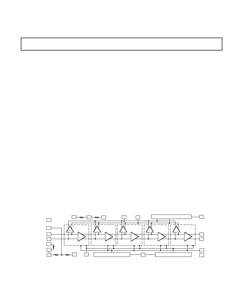
PRODUCT DESCRIPTION
The AD640 is a complete monolithic logarithmic amplifier. A single
AD640 provides up to 50 dB of dynamic range for frequencies
from dc to 120 MHz. Two AD640s in cascade can provide up to
95 dB of dynamic range at reduced bandwidth. The AD640 uses a
successive detection scheme to provide an output current propor-
tional to the logarithm of the input voltage. It is laser calibrated to
close tolerances and maintains high accuracy over the full military
temperature range using supply voltages from
±4.5 V to ±7.5 V.
The AD640 comprises five cascaded dc-coupled amplifier/limiter
stages, each having a small signal voltage gain of 10 dB and a –3 dB
bandwidth of 350 MHz. Each stage has an associated full-wave
detector, whose output current depends on the absolute value of its
input voltage. The five outputs are summed to provide the video
output (when low-pass filtered) scaled at 1 mA per decade (50
A
per dB). On chip resistors can be used to convert this output cur-
rent to a voltage with several convenient slope options. A balanced
signal output at +50 dB (referred to input) is provided to operate
AD640s in cascade.
The logarithmic response is absolutely calibrated to within
±1 dB
for dc or square wave inputs from
±0.75 mV to ±200 mV, with
an intercept (logarithmic offset) at 1 mV dc. An integral X10
attenuator provides an alternative input range of
±7.5 mV to
±2 V dc. Scaling is also guaranteed for sinusoidal inputs.
The AD640B is specified for the industrial temperature range of
–40
°C to +85°C and the AD640T, available processed to MIL-
STD-883B, for the military range of –55
°C to +125°C. Both are
available in 20-lead side-brazed ceramic DIPs or leadless chip
carriers (LCC). The AD640J is specified for the commercial
temperature range of 0
°C to +70°C, and is available in both
20-lead plastic DIP (N) and PLCC (P) packages.
This device is now available to Standard Military Drawing
(DESC) number 5962-9095501MRA and 5962-9095501M2A.
PRODUCT HIGHLIGHTS
1. Absolute calibration of a wideband logarithmic amplifier is
unique. The AD640 is a high accuracy measurement device,
not simply a logarithmic building block.
2. Advanced design results in unprecedented stability over the
full military temperature range.
3. The fully differential signal path greatly reduces the risk of
instability due to inadequate power supply decoupling and
shared ground connections, a serious problem with com-
monly used unbalanced designs.
4. Differential interfaces also ensure that the appropriate ground
connection can be chosen for each signal port. They further
increase versatility and simplify applications. The signal input
impedance is ~500 k
in shunt with ~2 pF.
5. The dc-coupled signal path eliminates the need for numerous
interstage coupling capacitors and simplifies logarithmic
conversion of subsonic signals.
(continued on page 4)
FUNCTIONAL BLOCK DIAGRAM
REV. C
Information furnished by Analog Devices is believed to be accurate and
reliable. However, no responsibility is assumed by Analog Devices for its
use, nor for any infringements of patents or other rights of third parties
which may result from its use. No license is granted by implication or
otherwise under any patent or patent rights of Analog Devices.
相关PDF资料 |
PDF描述 |
|---|---|
| 76382-320 | CONN HEADER 20POS .100" R/A GOLD |
| 65863-197 | QKE HDR 2X17 |
| 3408-6302 | CONN HEADER 16POS STR LONG LATCH |
| 3408-6202 | CONN HEADER 16PS STR SHORT LATCH |
| 3408-5602 | CONN HEADER 16POS R/A LONG LATCH |
相关代理商/技术参数 |
参数描述 |
|---|---|
| AD640JPZ-REEL7 | 功能描述:IC AMP LOG 2.3MA 20PLCC RoHS:是 类别:集成电路 (IC) >> Linear - Amplifiers - Instrumentation 系列:- 标准包装:50 系列:- 放大器类型:J-FET 电路数:2 输出类型:- 转换速率:3.5 V/µs 增益带宽积:1MHz -3db带宽:- 电流 - 输入偏压:30pA 电压 - 输入偏移:2000µV 电流 - 电源:200µA 电流 - 输出 / 通道:- 电压 - 电源,单路/双路(±):7 V ~ 36 V,±3.5 V ~ 18 V 工作温度:0°C ~ 70°C 安装类型:通孔 封装/外壳:8-DIP(0.300",7.62mm) 供应商设备封装:8-PDIP 包装:管件 |
| AD640T | 制造商:AD 制造商全称:Analog Devices 功能描述:DC-Coupled Demodulating 120 MHz Logarithmic Amplifier |
| AD640TCHIPS | 制造商:AD 制造商全称:Analog Devices 功能描述:DC-Coupled Demodulating 120 MHz Logarithmic Amplifier |
| AD640TD | 制造商:AD 制造商全称:Analog Devices 功能描述:DC-Coupled Demodulating 120 MHz Logarithmic Amplifier |
| AD640TD/883B | 功能描述:对数放大器 I.C. LOG AMP IC RoHS:否 制造商:Texas Instruments 通道数量:3 带宽:3 dB 共模抑制比(最小值): 输入补偿电压:+/- 7 mV 输入电压范围(最大值):5.5 V 工作电源电压:4.5 V to 5.5 V 电源电流:+/- 15 mA 工作温度范围:- 40 C to +85 C 安装风格:SMD/SMT 封装 / 箱体:VQFN-16 封装:Reel |
发布紧急采购,3分钟左右您将得到回复。