- 您现在的位置:买卖IC网 > PDF目录373890 > AD648AH (ANALOG DEVICES INC) Dual Precision, Low Power BiFET Op Amp PDF资料下载
参数资料
| 型号: | AD648AH |
| 厂商: | ANALOG DEVICES INC |
| 元件分类: | 运动控制电子 |
| 英文描述: | Dual Precision, Low Power BiFET Op Amp |
| 中文描述: | DUAL OP-AMP, 3000 uV OFFSET-MAX, 1 MHz BAND WIDTH, MBCY8 |
| 封装: | HERMETIC SEALED, METAL CAN, TO-99, 8 PIN |
| 文件页数: | 10/12页 |
| 文件大小: | 335K |
| 代理商: | AD648AH |
AD648
REV. C
–10–
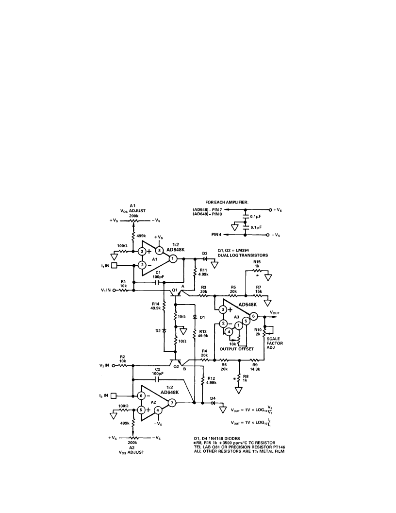
LOG RAT IO AMPLIFIE R
Log ratio amplifiers are useful for a variety of signal condition-
ing applications, such as linearizing exponential transducer out-
puts and compressing analog signals having a wide dynamic
range. T he AD648’s picoamp level input current and low input
offset voltage make it a good choice for the front-end amplifier
of the log ratio circuit shown in Figure 30. T his circuit produces
an output voltage equal to the log base 10 of the ratio of the in-
put currents I
1
and I
2
. Resistive inputs R1 and R2 are provided
for voltage inputs.
Input currents I
1
and I
2
set the collector currents of Q1 and Q2,
a matched pair of logging transistors. Voltages at points A and B
are developed according to the following familiar diode equation:
V
BE
=
(
kT/q
)
ln
(
I
C
/
I
ES
)
In this equation, k is Boltzmann’s constant, T is absolute tem-
perature, q is an electron charge, and I
ES
is the reverse satura-
tion current of the logging transistors. T he difference of these
two voltages is taken by the subtractor section and scaled by a
factor of approximately 16 by resistors R9, R10 and R8. T em-
perature compensation is provided by resistors R8 and R15,
which have a positive 3500 ppm/
°
C temperature coefficient.
T he transfer function for the output voltage is:
V
OUT
=
1
V log
10
(I
2
/I
1
)
Frequency compensation is provided by R11, R12, C1, and C2.
Small signal bandwidth is approximately 300 kHz at input cur-
rents above 100
μ
A and will proportionally decrease with lower
signal levels. D1, D2, R13, and R14 compensate for the effects
of the two logging transistors’ ohmic emitter resistance.
T o trim this circuit, set the two input currents to 10
μ
A and ad-
just V
OUT
to zero by adjusting the potentiometer on A3. T hen
set I
2
to 1
μ
A and adjust the scale factor such that the output
voltage is 1 V by trimming potentiometer R10. Offset adjust-
ment for A1 and A2 is provided to increase the accuracy of the
voltage inputs.
T his circuit ensures a 1% log conformance error over an input
current range of 300 pA to l mA, with low level accuracy limited
by the AD648’s input current. T he low level input voltage accu-
racy of this circuit is limited by the input offset voltage and drift
of the AD648.
Figure 30. Precision Log Ratio Amplifier
相关PDF资料 |
PDF描述 |
|---|---|
| AD648AQ | Dual Precision, Low Power BiFET Op Amp |
| AD648B | Dual Precision, Low Power BiFET Op Amp |
| AD648BH | Dual Precision, Low Power BiFET Op Amp |
| AD648BQ | Dual Precision, Low Power BiFET Op Amp |
| AD648C | Dual Precision, Low Power BiFET Op Amp |
相关代理商/技术参数 |
参数描述 |
|---|---|
| AD648AQ | 制造商:Rochester Electronics LLC 功能描述:LOW POWER DUAL OP AMP IC - Bulk |
| AD648B | 制造商:AD 制造商全称:Analog Devices 功能描述:Dual Precision, Low Power BiFET Op Amp |
| AD648BH | 制造商:Rochester Electronics LLC 功能描述:LOW POWER DUAL OP AMP IC - Bulk 制造商:Analog Devices 功能描述: |
| AD648BQ | 制造商:AD 制造商全称:Analog Devices 功能描述:Dual Precision, Low Power BiFET Op Amp |
| AD648C | 制造商:AD 制造商全称:Analog Devices 功能描述:Dual Precision, Low Power BiFET Op Amp |
发布紧急采购,3分钟左右您将得到回复。