- 您现在的位置:买卖IC网 > PDF目录373890 > AD648JCHIPS (ANALOG DEVICES INC) Dual Precision, Low Power BiFET Op Amp PDF资料下载
参数资料
| 型号: | AD648JCHIPS |
| 厂商: | ANALOG DEVICES INC |
| 元件分类: | 运动控制电子 |
| 英文描述: | Dual Precision, Low Power BiFET Op Amp |
| 中文描述: | DUAL OP-AMP, 3000 uV OFFSET-MAX, 1 MHz BAND WIDTH, UUC |
| 封装: | DIE |
| 文件页数: | 1/12页 |
| 文件大小: | 335K |
| 代理商: | AD648JCHIPS |
REV. C
Information furnished by Analog Devices is believed to be accurate and
reliable. However, no responsibility is assumed by Analog Devices for its
use, nor for any infringements of patents or other rights of third parties
which may result from its use. No license is granted by implication or
otherwise under any patent or patent rights of Analog Devices.
a
Dual Precision,
LowPower BiFET Op Amp
AD648
One Technology Way, P.O. Box 9106, Norwood, MA 02062-9106, U.S.A.
Tel: 617/329-4700
Fax: 617/326-8703
FEATURES
DC Performance
400
m
A max Quiescent Current
10 pA max Bias Current, Warmed Up (AD648C)
300
m
V max Offset Voltage (AD648C)
3
m
V/
8
C max Drift (AD648C)
2
m
V p-p Noise, 0.1 Hz to 10 Hz
AC Performance
1.8 V/
m
s Slew Rate
1 MHz Unity Gain Bandwidth
Available in Plastic Mini-DIP, Cerdip, Plastic SOIC
and Hermetic Metal Can Packages
MIL-STD-883B Parts Available
Surface Mount (SOIC) Package Available in Tape and
Reel in Accordance with EIA-481A Standard
Single Version: AD548
PRODUCT DE SCRIPT ION
T he AD648 is a matched pair of low power, precision mono-
lithic operational amplifiers. It offers both low bias current
(10 pA max, warmed up) and low quiescent current (400
μ
A
max) and is fabricated with ion-implanted FET and laser wafer
trimming technologies. Input bias current is guaranteed over the
AD648’s entire common-mode voltage range.
T he economical J grade has a maximum guaranteed offset volt-
age of less than 2 mV and an offset voltage drift of less than
20
μ
V/
°
C. T he C grade reduces offset voltage to less than
0.30 mV and offset voltage drift to less than 3
μ
V/
°
C. T his level
of dc precision is achieved utilizing Analog’s laser wafer drift
trimming process. T he combination of low quiescent current
and low offset voltage drift minimizes changes in input offset
voltage due to self-heating effects. Five additional grades are
offered over the commercial, industrial and military temperature
ranges.
T he AD648 is recommended for any dual supply op amp appli-
cation requiring low power and excellent dc and ac perfor-
mance. In applications such as battery-powered, precision
instrument front ends and CMOS DAC buffers, the AD648’s
excellent combination of low input offset voltage and drift, low
bias current and low 1/f noise reduces output errors. High
common-mode rejection (86 dB, min on the “C” grade) and
high open-loop gain ensures better than 12-bit linearity in high
impedance, buffer applications.
T he AD648 is pinned out in a standard dual op amp configura-
tion and is available in seven performance grades. T he AD648J
and AD648K are rated over the commercial temperature range
of 0
°
C to +70
°
C. T he AD648A, AD648B and AD648C are
rated over the industrial temperature range of –40
°
C to +85
°
C.
T he AD648S and AD648T are rated over the military tempera-
ture range of –55
°
C to +125
°
C and are available processed to
MIL-ST D-883B, Rev. C.
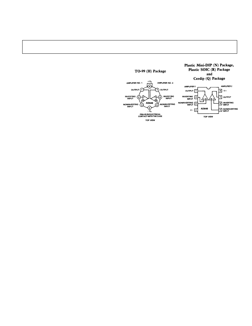
T he AD648 is available in an 8-pin plastic mini-DIP, cerdip,
SOIC, T O-99 metal can, or in chip form.
PRODUCT HIGHLIGHT S
1. A combination of low supply current, excellent dc and ac
performance and low drift makes the AD648 the ideal op
amp for high performance, low power applications.
2. T he AD648 is pin compatible with industry standard dual op
amps such as the LF442, T L062, and AD642, enabling
designers to improve performance while achieving a reduc-
tion in power dissipation of up to 85%.
3. Guaranteed low input offset voltage (2 mV max) and drift
(20
μ
V/
°
C max) for the AD648J are achieved utilizing Analog
Devices’ laser drift trimming technology.
4. Analog Devices specifies each device in the warmed-up con-
dition, insuring that the device will meet its published specifi-
cations in actual use.
5. Matching characteristics are excellent for all grades. T he
input offset voltage matching between amplifiers in the
AD648J is within 2 mV, for the C grade matching is within
0.4 mV.
6. Crosstalk between amplifiers is less than –120 dB at 1 kHz.
7. T he AD648 is available in chip form.
CONNE CT ION DIAGRAMS
相关PDF资料 |
PDF描述 |
|---|---|
| AD6526 | GSM/GPRS Digital Baseband Processor |
| AD654 | Low Cost Monolithic Voltage-to-Frequency Converter(低成本单片电压-频率转换器) |
| AD6600 | Dual Channel, Gain-Ranging ADC with RSSI |
| AD6600AST | Dual Channel, Gain-Ranging ADC with RSSI |
| AD6600PCB | Dual Channel, Gain-Ranging ADC with RSSI |
相关代理商/技术参数 |
参数描述 |
|---|---|
| AD648JN | 制造商:Rochester Electronics LLC 功能描述:LOW POWER DUAL OP AMP IC - Bulk 制造商:Analog Devices 功能描述:IC OP AMP DUAL BIFET DIP8 648 |
| AD648JNZ | 功能描述:IC OPAMP BIFET 1MHZ DUAL LP 8DIP RoHS:是 类别:集成电路 (IC) >> Linear - Amplifiers - Instrumentation 系列:- 产品培训模块:Differential Circuit Design Techniques for Communication Applications 标准包装:1 系列:- 放大器类型:RF/IF 差分 电路数:1 输出类型:差分 转换速率:9800 V/µs 增益带宽积:- -3db带宽:2.9GHz 电流 - 输入偏压:3µA 电压 - 输入偏移:- 电流 - 电源:40mA 电流 - 输出 / 通道:- 电压 - 电源,单路/双路(±):3 V ~ 3.6 V 工作温度:-40°C ~ 85°C 安装类型:表面贴装 封装/外壳:16-VQFN 裸露焊盘,CSP 供应商设备封装:16-LFCSP-VQ 包装:剪切带 (CT) 产品目录页面:551 (CN2011-ZH PDF) 其它名称:ADL5561ACPZ-R7CT |
| AD648JNZKL1 | 制造商:Rochester Electronics LLC 功能描述: 制造商:Analog Devices 功能描述: |
| AD648JR | 制造商:Analog Devices 功能描述:OP Amp Dual GP ±18V 8-Pin SOIC N 制造商:Rochester Electronics LLC 功能描述:LOW POWER DUAL OP AMP IC - Bulk 制造商:Analog Devices 功能描述:IC OP-AMP DUAL BIFET |
| AD648JR-REEL | 制造商:Analog Devices 功能描述:OP Amp Dual GP ±18V 8-Pin SOIC N T/R |
发布紧急采购,3分钟左右您将得到回复。