- 您现在的位置:买卖IC网 > PDF目录373890 > AD648KN (ANALOG DEVICES INC) Dual Precision, Low Power BiFET Op Amp PDF资料下载
参数资料
| 型号: | AD648KN |
| 厂商: | ANALOG DEVICES INC |
| 元件分类: | 运动控制电子 |
| 英文描述: | Dual Precision, Low Power BiFET Op Amp |
| 中文描述: | DUAL OP-AMP, 1500 uV OFFSET-MAX, 1 MHz BAND WIDTH, PDIP8 |
| 封装: | MINI, PLASTIC, DIP-8 |
| 文件页数: | 7/12页 |
| 文件大小: | 335K |
| 代理商: | AD648KN |
AD648
REV. C
–7–
SIGN BIT
BINARY NUMBER IN DAC REGISTER ANALOG OUTPUT
0
0
1
1
1111 1111 1111
0000 0000 0000
0000 0000 0000
1111 1111 1111
+V
IN
3
(4095/4096)
0 VOLTS
0 VOLTS
–V
IN
3
(4095/4096)
NOTE: SIGN BIT AT "0" CONNECTS THE NONINVERTING INPUT OF
A2 TO ANALOG COMMON
Figure 25. Sign Magnitude Code Table
Figure 23c shows a diode clamp protection scheme for an I-to-V
converter using low leakage diodes. Because the diodes are con-
nected to the op amp’s summing junction, which is a virtual
ground, their leakage contribution is minimal.
Figure 23c. I-to-V Converter with Diode Input Protection
Exceeding the negative common-mode range on either input
terminal causes a phase reversal at the output, forcing the ampli-
fier output to the corresponding high or low state. Exceeding
the negative common mode on both inputs simultaneously
forces the output high. Exceeding the positive common-mode
range on a single input doesn’t cause a phase reversal; but if
both inputs exceed the limit, the output will be forced high. In
all cases, normal amplifier operation is resumed when input
voltages are brought back within the common-mode range.
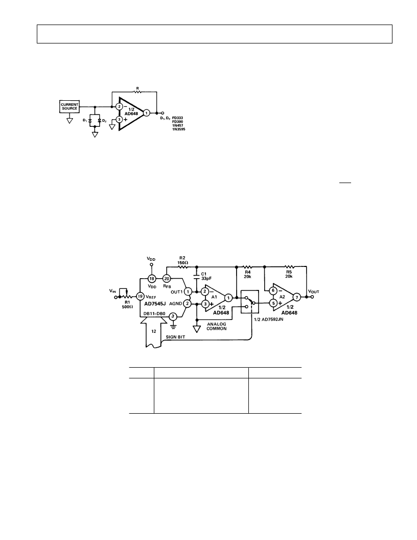
D/A CONVE RT E R BIPOLAR OUT PUT BUFFE R
T he circuit in Figure 24 provides 4 quadrant multiplication with
a resolution of 12 bits. T he AD648 is used to convert the AD7545
CMOS DAC’s output current to a voltage and provides the
necessary level shifting to achieve a bipolar voltage output. T he
circuit operates with a 12-bit plus sign input code. T he transfer
function is shown in Figure 25.
T he AD7592 is a fully protected dual CMOS SPDT switch with
data latches. R4 and R5 should match to within 0.01% to main-
tain the accuracy of the converter. A mismatch between R4 and
R5 introduces a gain error. Overall gain is trimmed by adjusting
R
IN
. T he AD648’s low input offset voltage, low drift over tem-
perature, and excellent dynamics make it an attractive low
power output buffer.
T he input offset voltage of the AD648 output amplifier results
in an output error voltage. T his error voltage equals the input
offset voltage of the op amp times the noise gain of the amplifier.
T hat is:
V
OS
Output
=
V
OS
Input
1
+
R
FB
R
O
R
FB
is the feedback resistor for the op amp, which is internal to
the DAC. R
O
is the DAC’s R-2R ladder output resistance. T he
value of R
O
is code dependent. T his has the effect of changing
the offset error voltage at the amplifier’s output. An output am-
plifier with a sub millivolt input offset voltage is needed to pre-
serve the linearity of the DAC’s transfer function.
Figure 24. 12-Bit Plus Sign Magnitude D/A Converter
相关PDF资料 |
PDF描述 |
|---|---|
| AD648KR | Dual Precision, Low Power BiFET Op Amp |
| AD648S | Dual Precision, Low Power BiFET Op Amp |
| AD648SQ | Dual Precision, Low Power BiFET Op Amp |
| AD648T | Dual Precision, Low Power BiFET Op Amp |
| AD648SCHIPS | Dual Precision, Low Power BiFET Op Amp |
相关代理商/技术参数 |
参数描述 |
|---|---|
| AD648KN/+ | 制造商:未知厂家 制造商全称:未知厂家 功能描述:Operational Amplifier |
| AD648KNZ | 功能描述:IC OPAMP BIFET 1MHZ DUAL LP 8DIP RoHS:是 类别:集成电路 (IC) >> Linear - Amplifiers - Instrumentation 系列:- 标准包装:2,500 系列:- 放大器类型:通用 电路数:4 输出类型:- 转换速率:0.6 V/µs 增益带宽积:1MHz -3db带宽:- 电流 - 输入偏压:45nA 电压 - 输入偏移:2000µV 电流 - 电源:1.4mA 电流 - 输出 / 通道:40mA 电压 - 电源,单路/双路(±):3 V ~ 32 V,±1.5 V ~ 16 V 工作温度:0°C ~ 70°C 安装类型:表面贴装 封装/外壳:14-TSSOP(0.173",4.40mm 宽) 供应商设备封装:14-TSSOP 包装:带卷 (TR) 其它名称:LM324ADTBR2G-NDLM324ADTBR2GOSTR |
| AD648KR | 制造商:Analog Devices 功能描述:OP Amp Dual GP ±18V 8-Pin SOIC N 制造商:Rochester Electronics LLC 功能描述:LOW POWER DUAL OP AMP IC - Bulk |
| AD648KR-REEL | 制造商:Analog Devices 功能描述:OP Amp Dual GP ±18V 8-Pin SOIC N T/R |
| AD648KR-REEL7 | 制造商:Analog Devices 功能描述:OP Amp Dual GP ±18V 8-Pin SOIC N T/R 制造商:Rochester Electronics LLC 功能描述:DUAL BIFET OP AMP IC - Tape and Reel |
发布紧急采购,3分钟左右您将得到回复。