参数资料
| 型号: | AD648KNZ |
| 厂商: | Analog Devices Inc |
| 文件页数: | 11/12页 |
| 文件大小: | 0K |
| 描述: | IC OPAMP BIFET 1MHZ DUAL LP 8DIP |
| 标准包装: | 50 |
| 放大器类型: | J-FET |
| 电路数: | 2 |
| 转换速率: | 1.8 V/µs |
| 增益带宽积: | 1MHz |
| 电流 - 输入偏压: | 3pA |
| 电压 - 输入偏移: | 300µV |
| 电流 - 电源: | 340µA |
| 电流 - 输出 / 通道: | 15mA |
| 电压 - 电源,单路/双路(±): | ±4.5 V ~ 18 V |
| 工作温度: | 0°C ~ 70°C |
| 安装类型: | 通孔 |
| 封装/外壳: | 8-DIP(0.300",7.62mm) |
| 供应商设备封装: | 8-PDIP |
| 包装: | 管件 |
| 产品目录页面: | 773 (CN2011-ZH PDF) |
AD648
REV. E
–8–
SIGN BIT
BINARY NUMBER IN DAC REGISTER ANALOG OUTPUT
0
1111 1111 1111
+VIN
(4095/4096)
0
0000 0000 0000
0 V
1
0000 0000 0000
0 V
1
1111 1111 1111
–VIN
(4095/4096)
NOTE
SIGN BIT AT “0“ CONNECTS THE NONINVERTING INPUT OF
A2 TO ANALOG COMMON
Figure 25. Sign Magnitude Code Table
Figure 23c shows a diode clamp protection scheme for an I-to-V
converter using low leakage diodes. Because the diodes are
connected to the op amp’s summing junction, which is a virtual
ground, their leakage contribution is minimal.
Figure 23c. I-to-V Converter with Diode Input Protection
Exceeding the negative common-mode range on either input
terminal causes a phase reversal at the output, forcing the ampli-
fier output to the corresponding high or low state. Exceeding
the negative common mode on both inputs simultaneously
forces the output high. Exceeding the positive common-mode
range on a single input does not cause a phase reversal; but if
both inputs exceed the limit, the output will be forced high. In
all cases, normal amplifier operation is resumed when input
voltages are brought back within the common-mode range.
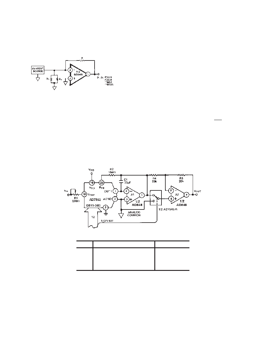
D/A CONVERTER BIPOLAR OUTPUT BUFFER
The circuit in Figure 24 provides 4 quadrant multiplication with
a resolution of 12 bits. The AD648 is used to convert the AD7545
CMOS DAC’s output current to a voltage and provides the
necessary level shifting to achieve a bipolar voltage output. The
circuit operates with a 12-bit plus sign input code. The transfer
function is shown in Figure 25.
The AD7592 is a fully protected dual CMOS SPDT switch with
data latches. R4 and R5 should match to within 0.01% to main-
tain the accuracy of the converter. A mismatch between R4 and
R5 introduces a gain error. Overall gain is trimmed by adjusting
RIN. The AD648’s low input offset voltage, low drift over tem-
perature, and excellent dynamics make it an attractive low
power output buffer.
The input offset voltage of the AD648 output amplifier results
in an output error voltage. This error voltage equals the input
offset voltage of the op amp times the noise gain of the amplifier.
That is:
VOS Output
= VOS Input 1+
RFB
RO
RFB is the feedback resistor for the op amp, which is internal to
the DAC. RO is the DAC’s R-2R ladder output resistance. The
value of RO is code dependent. This has the effect of changing
the offset error voltage at the amplifier’s output. An output
amplifier with a sub millivolt input offset voltage is needed to
preserve the linearity of the DAC’s transfer function.
Figure 24. 12-Bit Plus Sign Magnitude D/A Converter
相关PDF资料 |
PDF描述 |
|---|---|
| SMP04ESZ | IC AMP SAMPLE HOLD CMOS 16SOIC |
| TSW-102-07-G-D | CONN HEADER 4POS .100" DUAL GOLD |
| 929834-03-15-RK | CONN HEADER .100 SNGL STR 15POS |
| 929550-01-06-EU | CONN HEADER .100 SNGL R/A 6POS |
| 929834-04-11 | CONN HEADER .100 SNGL STR 11POS |
相关代理商/技术参数 |
参数描述 |
|---|---|
| AD648KR | 制造商:Analog Devices 功能描述:OP Amp Dual GP ±18V 8-Pin SOIC N 制造商:Rochester Electronics LLC 功能描述:LOW POWER DUAL OP AMP IC - Bulk |
| AD648KR-REEL | 制造商:Analog Devices 功能描述:OP Amp Dual GP ±18V 8-Pin SOIC N T/R |
| AD648KR-REEL7 | 制造商:Analog Devices 功能描述:OP Amp Dual GP ±18V 8-Pin SOIC N T/R 制造商:Rochester Electronics LLC 功能描述:DUAL BIFET OP AMP IC - Tape and Reel |
| AD648KRZ | 功能描述:IC OPAMP BIFET 1MHZ DUAL 8SOIC RoHS:是 类别:集成电路 (IC) >> Linear - Amplifiers - Instrumentation 系列:- 标准包装:1 系列:- 放大器类型:通用 电路数:4 输出类型:满摆幅 转换速率:0.028 V/µs 增益带宽积:105kHz -3db带宽:- 电流 - 输入偏压:3nA 电压 - 输入偏移:100µV 电流 - 电源:3.3µA 电流 - 输出 / 通道:12mA 电压 - 电源,单路/双路(±):2.7 V ~ 12 V,±1.35 V ~ 6 V 工作温度:-40°C ~ 85°C 安装类型:表面贴装 封装/外壳:14-TSSOP(0.173",4.40mm 宽) 供应商设备封装:14-TSSOP 包装:剪切带 (CT) 其它名称:OP481GRUZ-REELCT |
| AD648KRZ-REEL | 功能描述:IC OPAMP BIFET 1MHZ DUAL 8SOIC RoHS:是 类别:集成电路 (IC) >> Linear - Amplifiers - Instrumentation 系列:- 标准包装:150 系列:- 放大器类型:音频 电路数:2 输出类型:- 转换速率:5 V/µs 增益带宽积:12MHz -3db带宽:- 电流 - 输入偏压:100nA 电压 - 输入偏移:500µV 电流 - 电源:6mA 电流 - 输出 / 通道:50mA 电压 - 电源,单路/双路(±):4 V ~ 32 V,±2 V ~ 16 V 工作温度:-40°C ~ 85°C 安装类型:表面贴装 封装/外壳:8-TSSOP(0.173",4.40mm 宽) 供应商设备封装:8-TSSOP 包装:管件 |
发布紧急采购,3分钟左右您将得到回复。