参数资料
| 型号: | AD648KRZ-REEL |
| 厂商: | Analog Devices Inc |
| 文件页数: | 10/12页 |
| 文件大小: | 0K |
| 描述: | IC OPAMP BIFET 1MHZ DUAL 8SOIC |
| 标准包装: | 2,500 |
| 放大器类型: | J-FET |
| 电路数: | 2 |
| 转换速率: | 1.8 V/µs |
| 增益带宽积: | 1MHz |
| 电流 - 输入偏压: | 3pA |
| 电压 - 输入偏移: | 300µV |
| 电流 - 电源: | 340µA |
| 电流 - 输出 / 通道: | 15mA |
| 电压 - 电源,单路/双路(±): | ±4.5 V ~ 18 V |
| 工作温度: | 0°C ~ 70°C |
| 安装类型: | 表面贴装 |
| 封装/外壳: | 8-SOIC(0.154",3.90mm 宽) |
| 供应商设备封装: | 8-SO |
| 包装: | 带卷 (TR) |
AD648
REV. E
–7–
APPLICATION NOTES
The AD648 is a pair of JFET-input op amps with a guaranteed
maximum IB of less than 10 pA, and offset and drift laser-
trimmed to 1.0 mV and 10
V/°C, respectively (AD648B). AC
specs include 1 MHz bandwidth, 1.8 V/
s typical slew rate and
8
s settling time for a 20 V step to ±0.01%—all at a supply
current less than 400
A. To capitalize on the device’s perfor-
mance, a number of error sources should be considered.
The minimal power drain and low offset drift of the AD648
reduce self-heating or “warm-up” effects on input offset voltage,
making the AD648 ideal for on/off battery powered applica-
tions. The power dissipation due to the AD648’s 400
A supply
current has a negligible effect on input current, but heavy out-
put loading will raise the chip temperature. Since a JFET’s
input current doubles for every 10
°C rise in chip temperature,
this can be a noticeable effect.
The amplifier is designed to be functional with power supply
voltages as low as
±4.5 V. It will exhibit a higher input offset
voltage than at the rated supply voltage of
±15 V, due to power
supply rejection effects. Common-mode range extends from 3 V
more positive than the negative supply to 1 V more negative
than the positive supply. Designed to cleanly drive up to 10 k
and 100 pF loads, the AD648 will drive a 2 k
load with reduced
open-loop gain.
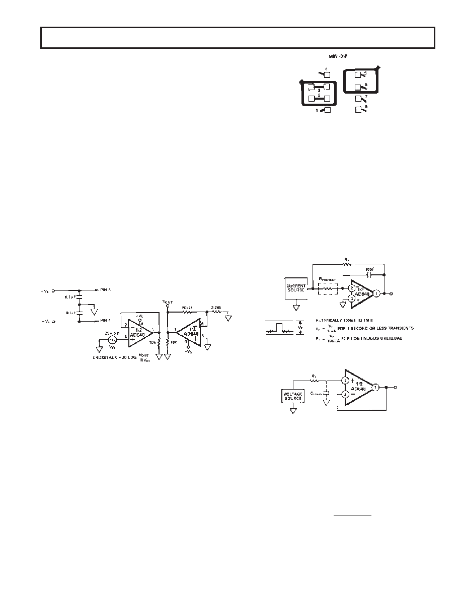
Figure 21 shows the recommended crosstalk test circuit. A
typical value for crosstalk is –120 dB at 1 kHz.
Figure 21. Crosstalk Test Circuit
LAYOUT
To take full advantage of the AD648’s 10 pA max input current,
parasitic leakages must be kept below an acceptable level. The
practical limit of the resistance of epoxy or phenolic circuit
board material is between 1
× 1012 and 3 × 10¹² . This can
result in an additional leakage of 5 pA between an input of 0 V
and a –15 V supply line. Teflon or a similar low leakage material
(with a resistance exceeding 10
17
) should be used to isolate
high impedance input lines from adjacent lines carrying high
voltages. The insulator should be kept clean, since contaminants
will degrade the surface resistance.
A metal guard completely surrounding the high impedance
nodes and driven by a voltage near the common-mode input
potential can also be used to reduce some parasitic leakages.
The guarding pattern in Figure 22 will reduce parasitic leakage
due to finite board surface resistance; but it will not compensate
for a low volume resistivity board.
Figure 22. Board Layout for Guarding Inputs
INPUT PROTECTION
The AD648 is guaranteed to withstand input voltages equal to
the power supply potential. Exceeding the negative supply volt-
age on either input will forward bias the substrate junction of
the chip. The induced current may destroy the amplifier due to
excess heat.
Input protection is required in applications such as a flame
detector in a gas chromatograph, where a very high potential
may be applied to the input terminals during a sensor fault
condition. Figures 23a and 23b show simple current limiting
schemes that can be used. RPROTECT should be chosen such that
the maximum overload current is 1.0 mA (for example 100 k
for a 100 V overload).
Figure 23a. Input Protection of l-to-V Converter
Figure 23b. Voltage Follower Input Protection Method
Figure 23b shows the recommended method for protecting a
voltage follower from excessive currents due to high voltage
breakdown. The protection resistor, RP, limits the input current.
A nominal value of 100 k
will limit the input current to less
than 1 mA with a 100 volt input voltage applied.
The stray capacitance between the summing junction and
ground will produce a high-frequency roll-off with a corner
frequency equal to:
fcorner
=
1
2
π RP Cstray
Accordingly, a 100 k
value for RP with a 3 pF Cstray will cause
a 3 dB corner frequency to occur at 531 kHz.
相关PDF资料 |
PDF描述 |
|---|---|
| MVU14-8FFBK | CONN TERM SPADE INS 16-14AWG #8 |
| MVU14-4FB/SK | CONN FORK INSUL 16-14 AWG #4 |
| MVU18-10FFBK | CONN TERM SPADE INS 22-18AWG #10 |
| MVU18-6FFBK | CONN TERM SPADE INS 22-18AWG #6 |
| MVU18-8FLK | CONN L/FORK INSUL 22-18 AWG #8 |
相关代理商/技术参数 |
参数描述 |
|---|---|
| AD648KRZ-REEL7 | 功能描述:IC OPAMP BIFET 1MHZ DUAL 8SOIC RoHS:是 类别:集成电路 (IC) >> Linear - Amplifiers - Instrumentation 系列:- 标准包装:150 系列:- 放大器类型:音频 电路数:2 输出类型:- 转换速率:5 V/µs 增益带宽积:12MHz -3db带宽:- 电流 - 输入偏压:100nA 电压 - 输入偏移:500µV 电流 - 电源:6mA 电流 - 输出 / 通道:50mA 电压 - 电源,单路/双路(±):4 V ~ 32 V,±2 V ~ 16 V 工作温度:-40°C ~ 85°C 安装类型:表面贴装 封装/外壳:8-TSSOP(0.173",4.40mm 宽) 供应商设备封装:8-TSSOP 包装:管件 |
| AD648S | 制造商:AD 制造商全称:Analog Devices 功能描述:Dual Precision, Low Power BiFET Op Amp |
| AD648SCHIPS | 制造商:AD 制造商全称:Analog Devices 功能描述:Dual Precision, Low Power BiFET Op Amp |
| AD648SH | 制造商:未知厂家 制造商全称:未知厂家 功能描述:Operational Amplifier |
| AD648SH/883B | 制造商:Rochester Electronics LLC 功能描述:- Bulk |
发布紧急采购,3分钟左右您将得到回复。