- 您现在的位置:买卖IC网 > PDF目录22156 > AD652KPZ (Analog Devices Inc)IV V-F CONVERTER SYNC 20-PLCC PDF资料下载
参数资料
| 型号: | AD652KPZ |
| 厂商: | Analog Devices Inc |
| 文件页数: | 7/28页 |
| 文件大小: | 779K |
| 描述: | IV V-F CONVERTER SYNC 20-PLCC |
| 标准包装: | 1 |
| 类型: | 电压至频率 |
| 频率 - 最大: | 2MHz |
| 全量程: | ±25ppm/°C |
| 线性: | ±0.005% |
| 安装类型: | 表面贴装 |
| 封装/外壳: | 20-LCC(J 形引线) |
| 供应商设备封装: | 20-PLCC(9x9) |
| 包装: | 管件 |
第1页第2页第3页第4页第5页第6页当前第7页第8页第9页第10页第11页第12页第13页第14页第15页第16页第17页第18页第19页第20页第21页第22页第23页第24页第25页第26页第27页第28页
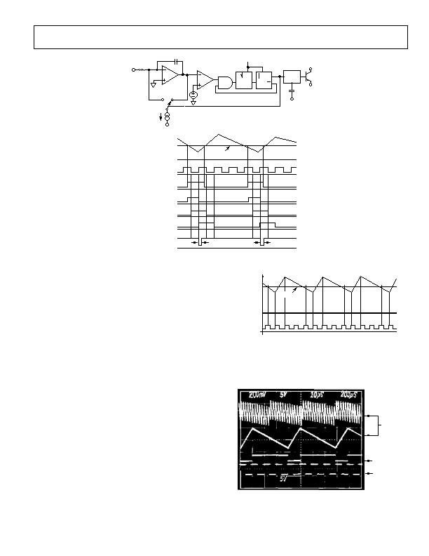
AD652
Rev. C | Page 7 of 28
COMPARATOR
AND
CK
Q
D
G
Q
D
Q
D FLOP
LATCH
CLOCK IN
ONE
SHOT
C
OS
5V
C
INT
R
IN
INTEGRATOR
H L
1mA
V
S
V
IN
t
OS
t
OS
INTEGRATOR
OUTPUT
THRESHOLD
CLOCK
COMPARATOR
OUT
AND
OUT
D FLOP
OUT
LATCH
OUT
FREQ
OUT
Figure 4. Block Diagram and System Waveforms
Figure 4 shows that the period between output pulses is
constrained to be an exact multiple of the clock period.
Consider an input current of exactly one quarter the value of
the reference current. In order to achieve a charge balance, the
output frequency equals the clock frequency divided by four:
one clock period for reset and three clock periods of integrate.
This is shown in Figure 5. If the input current is increased by a
very small amount, the output frequency should also increase
by a very small amount. Initially, however, no output change is
observed for a very small increase in the input current. The
output frequency continues to run at one quarter of the clock,
delivering an average of 250 礎 to the summing junction. Since
the input current is slightly larger than this, charge accumulates
in the integrator and the sawtooth signal starts to drift down-
ward. As the integrator sawtooth drifts down, the comparator
threshold is crossed earlier and earlier in each successive cycle,
until finally, a whole cycle is lost. When the cycle is lost, the
integrate phase lasts for two periods of the clock instead of the
usual three periods. Thus, among a long string of divide-by-
fours, an occasional divide-by-three occurs; the average of the
output frequency is very close to one quarter of the clock, but
the instantaneous frequency can be very different.
INTEGRATO
OUT
CLOCK
THRESHOLD
Figure 5. Integrator Output for I
IN
= 250 礎
Because of this, it is very difficult to observe the waveform on
an oscilloscope. During all of this time, the signal at the output
of the integrator is a sawtooth wave with an envelope that is also
a sawtooth. See Figure 6.
200?/SPAN>s/BOX
100?/SPAN>s/BOX
C
INT
FREQ OUT
10?/SPAN>s/BOX
CLOCK IN
10?/SPAN>s/BOX
Figure 6. Integrator Output for I
IN
Slightly Greater than 250 祍
相关PDF资料 |
PDF描述 |
|---|---|
| AD652KP | IV V-F CONVERTER SYNC 20-PLCC |
| RCC65DRAI | CONN EDGECARD 130PS R/A .100 SLD |
| RBB108DHFN | CONN EDGECARD 216POS .050 SMD |
| RBB108DHFD | CONN EDGECARD 216POS .050 SMD |
| AD650KN | IC V-F/F-V CONVERTER 14-DIP |
相关代理商/技术参数 |
参数描述 |
|---|---|
| AD652KPZ | 制造商:Analog Devices 功能描述:IC VOLTAGE CONVERTER |
| AD652KPZ-REEL | 功能描述:IC V-F CONVERTER SYNC 20PLCC RoHS:是 类别:集成电路 (IC) >> PMIC - V/F 和 F/V 转换器 系列:- 标准包装:1 系列:- 类型:频率至电压 频率 - 最大:10kHz 全量程:- 线性:±0.3% 安装类型:表面贴装 封装/外壳:8-SOIC(0.154",3.90mm 宽) 供应商设备封装:8-SOIC 包装:Digi-Reel® 其它名称:LM2917MX-8/NOPBDKR |
| AD652SE/883B | 功能描述:电压频率转换及频率电压转换 IC - SYNC V/F CONVERTER RoHS:否 制造商:Texas Instruments 全标度频率:4000 KHz 线性误差:+/- 1 % FSR 电源电压-最大: 电源电压-最小: 最大工作温度:+ 85 C 最小工作温度:- 25 C 安装风格:Through Hole 封装 / 箱体:PDIP-14 封装:Tube |
| AD652SE/883B2 | 制造商:AD 制造商全称:Analog Devices 功能描述:Monolithic Synchronous Voltage-to-Frequency Converter |
| AD652SE883B2 | 制造商:AD 制造商全称:Analog Devices 功能描述:Monolithic Synchronous Voltage-to-Frequency Converter |
发布紧急采购,3分钟左右您将得到回复。