- 您现在的位置:买卖IC网 > PDF目录373890 > AD660 (Analog Devices, Inc.) Monolithic 16-Bit Serial/Byte DACPORT(16位单片D/A转换器) PDF资料下载
参数资料
| 型号: | AD660 |
| 厂商: | Analog Devices, Inc. |
| 英文描述: | Monolithic 16-Bit Serial/Byte DACPORT(16位单片D/A转换器) |
| 中文描述: | 单片16位串行/字节DACPORT(16位单片的D / A转换器) |
| 文件页数: | 6/12页 |
| 文件大小: | 435K |
| 代理商: | AD660 |
AD660
REV. A
–6–
SIGNAL-TO-NOISE RATIO: The signal-to-noise ratio is de-
fined as the ratio of the amplitude of the output when a full-
scale signal is present to the output with no signal present. This
is measured in dB.
DIGITAL-TO-ANALOG GLITCH IMPULSE: This is the
amount of charge injected from the digital inputs to the analog
output when the inputs change state. This is measured at half
scale when the DAC switches around the MSB and as many
as possible switches change state, i.e., from 011 . . . 111 to
100 . . . 000.
DIGITAL FEEDTHROUGH: When the DAC is not selected
(i.e.,
CS
is held high), high frequency logic activity on the digi-
tal inputs is capacitively coupled through the device to show up
as noise on the V
OUT
pin. This noise is digital feedthrough.
THEORY OF OPERATION
The AD660 uses an array of bipolar current sources with MOS
current steering switches to develop a current proportional to
the applied digital word, ranging from 0 to 2 mA. A segmented
architecture is used, where the most significant four data bits are
thermometer decoded to drive 15 equal current sources. The
lesser bits are scaled using a R-2R ladder, then applied together
with the segmented sources to the summing node of the output
amplifier. The internal span/bipolar offset resistor can be con-
nected to the DAC output to provide a 0 V to +10 V span, or it
can be connected to the reference input to provide a –10 V to
+10 V span.
16-BIT LATCH
16-BIT DAC
CONTROL
LOGIC
+10V REF
16-BIT LATCH
20
24
22
21
5
11
12
16
15
14
13
17
18
19
23
AD660
10k
10.05k
10k
SIN/
DB0
DB7
S
OUT
SPAN/
BIP
OFFSET
V
OUT
AGND
REF OUT
REF IN
LDAC
SER
DGND
–V
EE
+V
CC
+V
LL
1
2
3
4
LBE
CS
HBE
CLR
MSB/LSB/
DB1
UNI/BIP CLR/
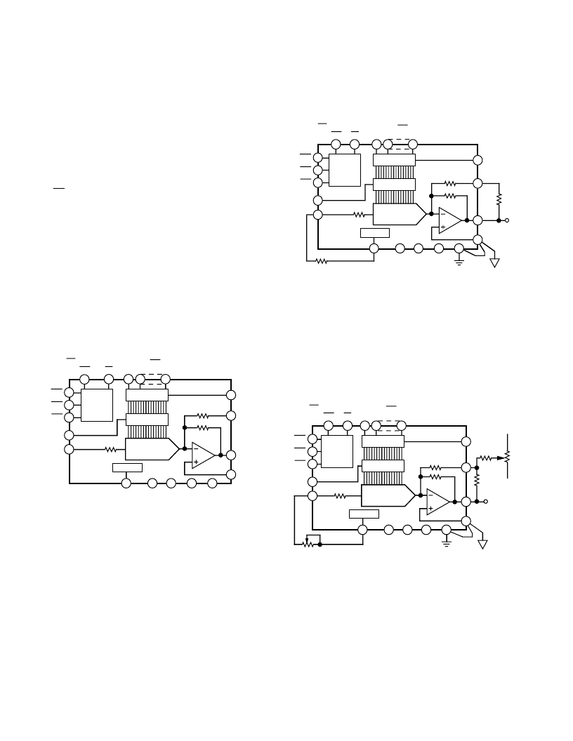
Figure 2. AD660 Functional Block Diagram
ANALOG CIRCUIT CONNECTIONS
Internal scaling resistors provided in the AD660 may be con-
nected to produce a unipolar output range of 0 V to +10 V or a
bipolar output range of –10 V to +10 V. Gain and offset drift
are minimized in the AD660 because of the thermal tracking of
the scaling resistors with other device components.
UNIPOLAR CONFIGURATION
The configuration shown in Figure 3a will provide a unipolar
0 V to +10 V output range. In this mode, 50
resistors are tied
between the span/bipolar offset terminal (Pin 22) and V
OUT
(Pin 21), and between REF OUT (Pin 24) and REF IN (Pin
23). It is possible to use the AD660 without any external compo-
nents by tying Pin 24 directly to Pin 23 and Pin 22 directly to
Pin 21. Eliminating these resistors will increase the gain error by
0.25% of FSR.
16-BIT LATCH
16-BIT DAC
CONTROL
LOGIC
+10V REF
16-BIT LATCH
20
24
22
21
5
11
12
16
15
14
13
17
18
19
23
AD660
10k
10.05k
10k
HBE
LBE
CS
SIN/
DB0
MSB/LSB/
DB1
DB7
S
OUT
SPAN/
BIP OFF
V
OUT
AGND
REF OUT
REF IN
LDAC
CLR
SER
DGND
–V
EE
+V
CC
+V
LL
1
2
3
4
R1 50
OUTPUT
R2
50
UNI/BIP CLR/
Figure 3a. 0 V to +10 V Unipolar Voltage Output
If it is desired to adjust the gain and offset errors to zero, this can
be accomplished using the circuit shown in Figure 3b. The ad-
justment procedure is as follows:
STEP 1 . . . ZERO ADJUST
Turn all bits OFF and adjust zero trimmer, R4, until the output
reads 0.000000 volts (1 LSB = 153
μ
V).
STEP 2 . . . GAIN ADJUST
Turn all bits ON and adjust gain trimmer, R1, until the output is
9.999847 volts. (Full scale is adjusted to 1 LSB less than the
nominal full scale of 10.000000 volts).
16-BIT LATCH
16-BIT DAC
CONTROL
LOGIC
+10V REF
16-BIT LATCH
20
24
22
21
5
11
12
16
15
14
13
17
18
19
23
AD660
10k
10.05k
10k
HBE
LBE
CS
SIN/
DB0
MSB/LSB/
DB1
DB7
S
OUT
SPAN/
BIP OFF
REF OUT
REF IN
LDAC
CLR
SER
DGND
–V
EE
+V
CC
+V
LL
1
2
3
4
OUTPUT
R2
50
R4
10k
+V
CC
–V
EE
R1 100
AGND
UNI/BIP CLR/
Figure 3b. 0 V to +10 V Unipolar Voltage Output with Gain
and Offset Adjustment
相关PDF资料 |
PDF描述 |
|---|---|
| AD6620PCB | 65 MSPS Digital Receive Signal Processor |
| AD6620AS | 65 MSPS Digital Receive Signal Processor |
| AD6620S | 65 MSPS Digital Receive Signal Processor |
| AD6620 | 65 MSPS Digital Receive Signal Processor(采样速率65MSPS的数字接收信号处理器) |
| AD6622AS | Four-Channel, 75 MSPS Digital Transmit Signal Processor TSP |
相关代理商/技术参数 |
参数描述 |
|---|---|
| AD660_08 | 制造商:AD 制造商全称:Analog Devices 功能描述:Monolithic 16-Bit Serial/Byte DACPORT |
| AD6600 | 制造商:AD 制造商全称:Analog Devices 功能描述:Dual Channel, Gain-Ranging ADC with RSSI |
| AD6600AST | 制造商:Analog Devices 功能描述:ADC Single 20Msps 11-bit Parallel 44-Pin LQFP 制造商:Rochester Electronics LLC 功能描述:DUAL CHANNEL GAIN RANGING ADS WITH RSSI - Tape and Reel |
| AD6600AST-REEL | 制造商:Analog Devices 功能描述:ADC Single 20Msps 11-bit Parallel 44-Pin LQFP T/R |
| AD6600ASTZ | 功能描述:IC ADC DUAL W/RSSI 44-LQFP RoHS:是 类别:集成电路 (IC) >> 数据采集 - 模数转换器 系列:- 标准包装:1 系列:- 位数:14 采样率(每秒):83k 数据接口:串行,并联 转换器数目:1 功率耗散(最大):95mW 电压电源:双 ± 工作温度:0°C ~ 70°C 安装类型:通孔 封装/外壳:28-DIP(0.600",15.24mm) 供应商设备封装:28-PDIP 包装:管件 输入数目和类型:1 个单端,双极 |
发布紧急采购,3分钟左右您将得到回复。