- 您现在的位置:买卖IC网 > PDF目录8564 > AD660BR-REEL (Analog Devices Inc)IC DAC 16BIT MONO W/VREF 24-SOIC PDF资料下载
参数资料
| 型号: | AD660BR-REEL |
| 厂商: | Analog Devices Inc |
| 文件页数: | 7/20页 |
| 文件大小: | 0K |
| 描述: | IC DAC 16BIT MONO W/VREF 24-SOIC |
| 产品培训模块: | Data Converter Fundamentals DAC Architectures |
| 标准包装: | 1,000 |
| 系列: | DACPORT® |
| 设置时间: | 6µs |
| 位数: | 16 |
| 数据接口: | 串行 |
| 转换器数目: | 1 |
| 电压电源: | 模拟和数字,双 ± |
| 功率耗散(最大): | 625mW |
| 工作温度: | -40°C ~ 85°C |
| 安装类型: | 表面贴装 |
| 封装/外壳: | 24-SOIC(0.295",7.50mm 宽) |
| 供应商设备封装: | 24-SOIC W |
| 包装: | 带卷 (TR) |
| 输出数目和类型: | 1 电压,单极;1 电压,双极 |
| 采样率(每秒): | 167k |
AD660
Rev. B | Page 15 of 20
MICROPROCESSOR INTERFACE
AD660 TO MC68HC11 (SPI BUS) INTERFACE
The AD660 interface to the Motorola SPI (serial peripheral
interface) is shown in Figure 17. The MOSI, SCK, and SS pins
of the 68HC11 are respectively connected to the DB0/DB8/SIN,
CS, and LDAC pins of the AD660. The SER pin of the AD660 is
tied low causing the first rank latch to be transparent. The
majority of the interfacing issues are taken care of in the
software initialization. A typical routine such as the one shown
in the Software Initialization Example begins by initializing the
state of the various SPI data and control registers.
The most significant data byte (MSBY) is then retrieved from
memory and processed by the SENDAT subroutine. The SS pin
is driven low by indexing into the PORTD data register and
clearing Bit 5. This causes the 2nd rank latch of the AD660 to
become transparent. The MSBY is then set to the SPI data
register where it is automatically transferred to the AD660.
The HC11 generates the requisite eight clock pulses with data
valid on the rising edges. After the most significant byte is
transmitted, the least significant byte (LSBY) is loaded from
memory and transmitted in a similar fashion. To complete the
transfer, the LDAC pin is driven high, latching the complete
16-bit word into the AD660.
Software Initialization Example
INIT
LDAA
#$2F
; SS = I; SCK = 0; MOSI
= I
STAA
PORTD
;SEND TO SPI OUTPUTS
LDAA
#$38
; SS, SCK,MOSI = OUTPUTS
STAA
DDRD
;SEND DATA DIRECTION
INFO
LDAA
#$50
;DABL INTRPTS,SPI IS
MASTER & ON
STAA
SPCR
;CPOL = 0, CPHA = 0,1MHZ
BAUD RATE
NEXTPT
LDAA
MSBY
;LOAD ACCUM WITH UPPER 8
BITS
BSR
SENDAT
;JUMP TO DAC OUTPUT
ROUTINE
JMP
NEXTPT
;INFINITE LOOP
SENDAT
LDY
#$1000
;POINT AT ON-CHIP
REGISTERS
BCLR
$08,Y,$20
;DRIVE SS (LDAC) LOW
STAA
SPDR
;SEND MS-BYTE TO SPI
DATA REG
WAIT1
LDAA
SPSR
;CHECK STATUS OF SPIE
BPL
WAIT1
;POLL FOR END OF X-
MISSION
LDAA
LSBY
;GET LOW 8 BITS FROM
MEMORY
STAA
SPDR
;SEND LS-BYTE TO SPI
DATA REG
WAIT2
LDAA
SPSR
;CHECK STATUS OF SPIE
BPL
WAIT2
;POLL FOR END OF X-
MISSION
BSET
$08,Y,$20
;DRIV SS HIGH TO LATCH
DATA
RTS
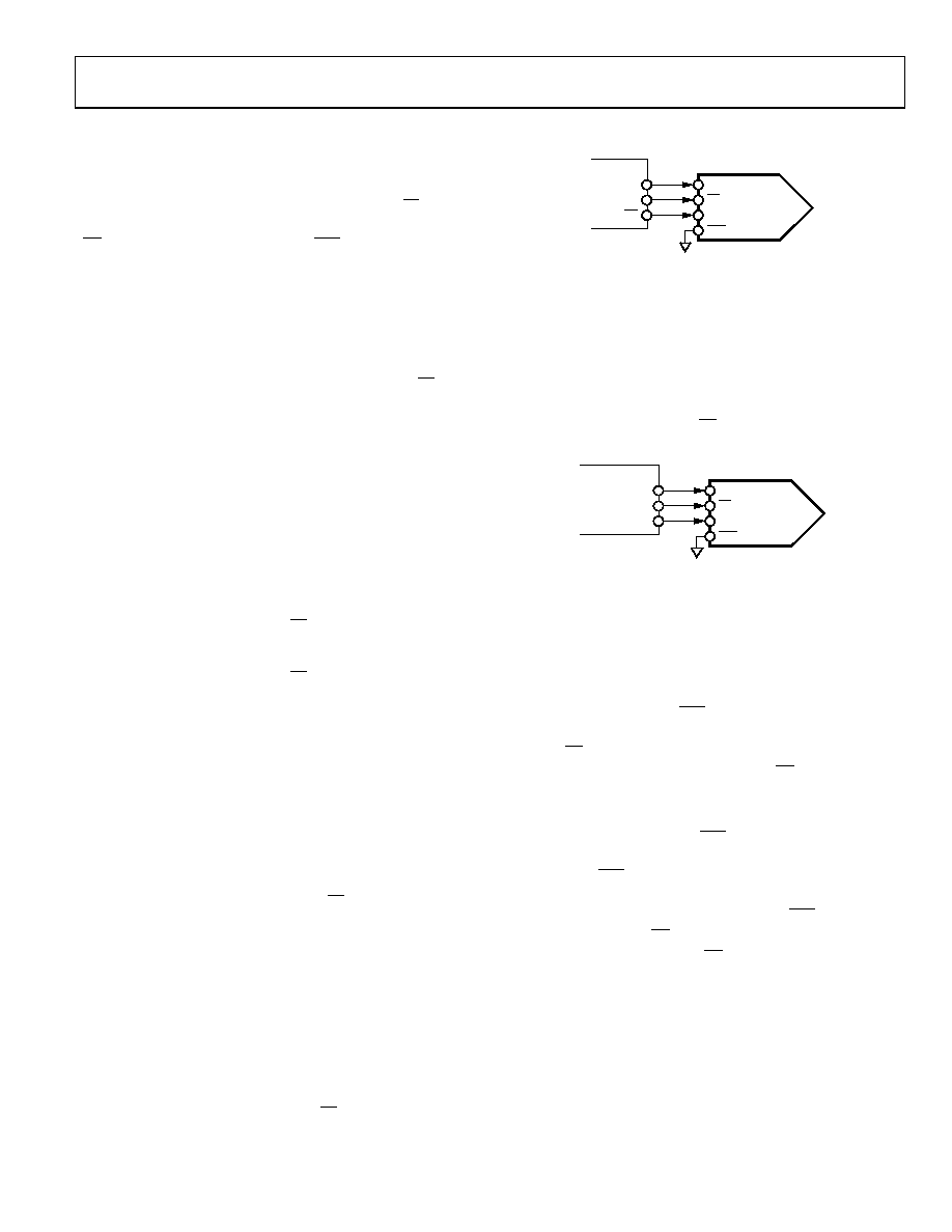
DB0/DB8/SIN
CS
LDAC
MDSI
SCK
SS
AD660
68HC11
SER
018
13
-01
7
Figure 17. AD660 to 68HC11 (SPI) Interface
AD660 TO MICROWIRE INTERFACE
The flexible serial interface of the AD660 is also compatible
with the National Semiconductor MICROWIRE interface.
The MICROWIRE interface is used on microcontrollers, such
as the COP400 and COP800 series of processors. A generic
interface to the MICROWIRE interface is shown in Figure 18.
The G1, SK, and SO pins of the MICROWIRE interface are respec-
tively connected to the LDAC, CS and DB0/DB8/SIN pins of
the AD660.
DB0/DB8/SIN
CS
LDAC
SO
SK
G1
AD660
MICROWIRE
SER
018
13
-01
8
Figure 18. AD660 to MICROWIRE Interface
AD660 TO ADSP-210x FAMILY INTERFACE
The serial mode of the AD660 minimizes the number of control
and data lines required to interface to digital signal processors
(DSPs) such as the ADSP-210x family. The application in
Figure 19 shows the interface between an ADSP-210x and the
AD660. Both the TFS pin and the DT pins of the ADSP-210x
should be connected to the SER and DB0 pins of the AD660,
respectively. An inverter is required between the SCLK output
and the CS input of the AD660 to ensure that data transmitted
to the DB0 pin is valid on the rising edge of CS.
The serial port (SPORT) of the DSP should be configured for
alternate framing mode so that TFS complies with the word
length framing requirement of SER. Note that the INVTFS bit
in the SPORT control register should be set to invert the TFS
signal so that SER is the correct polarity. The LDAC signal,
which must meet the minimum hold specification of tHIGH, is
easily generated by delaying the rising edge of SER with a
74HC74 flip-flop. The CS signal clocks the flip-flop, resulting
in a delay of approximately one CS clock cycle.
相关PDF资料 |
PDF描述 |
|---|---|
| LTC1592AIG#PBF | IC D/A CONV 16BIT SOFTSPAN16SSOP |
| LTC1592AIG | IC D/A CONV 16BIT SOFTSPAN16SSOP |
| AD5391BSTZ-5 | IC DAC 12BIT 16CHAN 3V 52LQFP |
| AD5391BSTZ-3 | IC DAC 12BIT 16CHAN 3V 52LQFP |
| AD5391BCPZ-5 | IC DAC 12BIT 16CH 5V 64-LFCSP |
相关代理商/技术参数 |
参数描述 |
|---|---|
| AD660BRZ | 功能描述:IC DAC 16BIT MONO W/VREF 24-SOIC RoHS:是 类别:集成电路 (IC) >> 数据采集 - 数模转换器 系列:DACPORT® 标准包装:1 系列:- 设置时间:4.5µs 位数:12 数据接口:串行,SPI? 转换器数目:1 电压电源:单电源 功率耗散(最大):- 工作温度:-40°C ~ 125°C 安装类型:表面贴装 封装/外壳:8-SOIC(0.154",3.90mm 宽) 供应商设备封装:8-SOICN 包装:剪切带 (CT) 输出数目和类型:1 电压,单极;1 电压,双极 采样率(每秒):* 其它名称:MCP4921T-E/SNCTMCP4921T-E/SNRCTMCP4921T-E/SNRCT-ND |
| AD660BRZ1 | 制造商:AD 制造商全称:Analog Devices 功能描述:Monolithic 16-Bit Serial/Byte DACPORT |
| AD660BRZ-REEL | 功能描述:IC DAC 16BIT MONO W/VREF 24-SOIC RoHS:是 类别:集成电路 (IC) >> 数据采集 - 数模转换器 系列:DACPORT® 产品培训模块:Data Converter Fundamentals DAC Architectures 标准包装:750 系列:- 设置时间:7µs 位数:16 数据接口:并联 转换器数目:1 电压电源:双 ± 功率耗散(最大):100mW 工作温度:0°C ~ 70°C 安装类型:表面贴装 封装/外壳:28-LCC(J 形引线) 供应商设备封装:28-PLCC(11.51x11.51) 包装:带卷 (TR) 输出数目和类型:1 电压,单极;1 电压,双极 采样率(每秒):143k |
| AD660BRZ-REEL1 | 制造商:AD 制造商全称:Analog Devices 功能描述:Monolithic 16-Bit Serial/Byte DACPORT |
| AD660KWOHLBOX | 制造商:Advanced Micro Devices 功能描述:AMD A-SERIES APU A8-6600K X4 BE 4300MHZ 4MB FM2 100W PIB - Boxed Product (Development Kits) |
发布紧急采购,3分钟左右您将得到回复。