- 您现在的位置:买卖IC网 > PDF目录8570 > AD660BRZ-REEL (Analog Devices Inc)IC DAC 16BIT MONO W/VREF 24-SOIC PDF资料下载
参数资料
| 型号: | AD660BRZ-REEL |
| 厂商: | Analog Devices Inc |
| 文件页数: | 1/20页 |
| 文件大小: | 0K |
| 描述: | IC DAC 16BIT MONO W/VREF 24-SOIC |
| 产品培训模块: | Data Converter Fundamentals DAC Architectures |
| 标准包装: | 1,000 |
| 系列: | DACPORT® |
| 设置时间: | 6µs |
| 位数: | 16 |
| 数据接口: | 串行 |
| 转换器数目: | 1 |
| 电压电源: | 模拟和数字,双 ± |
| 功率耗散(最大): | 625mW |
| 工作温度: | -40°C ~ 85°C |
| 安装类型: | 表面贴装 |
| 封装/外壳: | 24-SOIC(0.295",7.50mm 宽) |
| 供应商设备封装: | 24-SOIC W |
| 包装: | 带卷 (TR) |
| 输出数目和类型: | 1 电压,单极;1 电压,双极 |
| 采样率(每秒): | 167k |
Monolithic 16-Bit
Serial/Byte DACPORT
AD660
Rev. B
Information furnished by Analog Devices is believed to be accurate and reliable. However, no
responsibilityis assumedbyAnalogDevicesforitsuse,norforanyinfringementsof patentsorother
rightsofthirdpartiesthatmayresultfromitsuse.Specificationssubjecttochangewithoutnotice.No
license is granted by implication or otherwise under any patent or patent rights of Analog Devices.
Trademarksandregisteredtrademarksarethepropertyoftheirrespectiveowners.
One Technology Way, P.O. Box 9106, Norwood, MA 02062-9106, U.S.A.
Tel: 781.329.4700
www.analog.com
Fax: 781.461.3113
1993–2008 Analog Devices, Inc. All rights reserved.
FEATURES
Complete 16-bit digital-to-analog function
On-chip output amplifier
On-chip buried Zener voltage reference
±1 LSB integral linearity
15-bit monotonic over temperature
Microprocessor compatible
Serial or byte input
Double-buffered latches
Fast (40 ns) write pulse
Asynchronous clear (to 0 V) function
Serial output pin facilitates daisy-chaining
Unipolar or bipolar output
Low glitch: 15 nV-s
Low THD + N: 0.009%
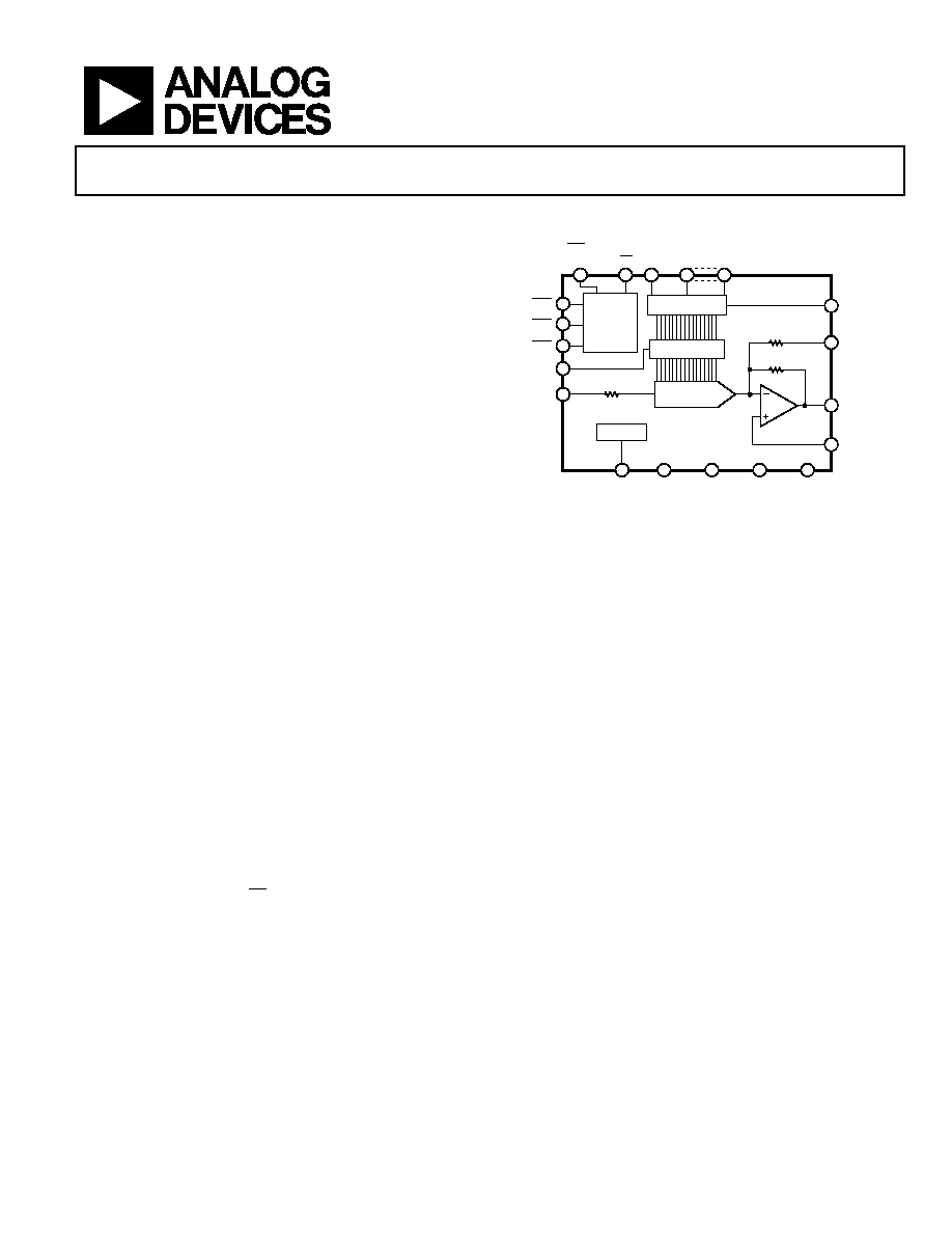
FUNCTIONAL BLOCK DIAGRAM
HBE
CONTROL
LOGIC
SER
CLR
LDAC
REF IN
10k
10.05k
REF OUT
CS
DB7/
DB15
AD660
SOUT
VOUT
AGND
SPAN/
BIPOLAR
OFFSET
DGND
–VEE
+VCC
+VLL
10V REF
16-BIT LATCH
16-BIT DAC
16-BIT LATCH
16
17
18
19
23
24
20
21
22
13
5
1
2
3
4
12
14
15
01
81
3-
0
01
DB1/DB9/
DATADIR
11
LBE/
CLEAR SELECT
DB0/
DB8/
SIN
Figure 1.
GENERAL DESCRIPTION
The AD660 DACPORT is a complete 16-bit monolithic digital-
to-analog converter with an on-board voltage reference, double-
buffered latches, and an output amplifier. It is manufactured on
the Analog Devices, Inc., BiMOS II process. This process allows
the fabrication of low power CMOS logic functions on the same
chip as high precision bipolar linear circuitry.
The AD660 architecture ensures 15-bit monotonicity over time
and temperature. Integral and differential nonlinearity is main-
tained at ±0.003% maximum. The on-chip output amplifier
provides a voltage output settling time of 10 μs to within LSB for
a full-scale step.
The AD660 has an extremely flexible digital interface. Data can
be loaded into the AD660 in serial mode or as two 8-bit bytes.
This is made possible by two digital input pins that have dual
functions. The serial mode input format is pin selectable to be
MSB or LSB first. The serial output pin allows the user to daisy-
chain several AD660 devices by shifting the data through the
input latch into the next DAC, thus minimizing the number of
control lines required to SIN, CS and LDAC. The byte mode input
format is also flexible in that the high byte or low byte data can
be loaded first. The double buffered latch structure eliminates
data skew errors and provides for simultaneous updating of DACs
in a multiDAC system.
The AD660 is available in five grades. AN and BN versions are
specified from 40°C to +85°C and are packaged in a 24-lead
300 mil plastic DIP. AR and BR versions are also specified from
40°C to +85°C and are packaged in a 24-lead SOIC. The SQ
version is packaged in a 24-lead 300 mil CERDIP package and
is also available compliant to MIL-STD-883. Refer to the
AD660SQ/883B military data sheet for specifications and test
conditions.
PRODUCT HIGHLIGHTS
1.
The AD660 is a complete 16-bit DAC, with a voltage
reference, double-buffered latches, and an output amplifier
on a single chip.
2.
The internal buried Zener reference is laser trimmed to
10.000 V with a ±0.1% maximum error and a temperature
drift performance of ±15 ppm/°C. The reference is available
for external applications.
3.
The output range of the AD660 is pin programmable and
can be set to provide a unipolar output range of 0 V to 10 V
or a bipolar output range of 10 V to +10 V. No external
components are required.
4.
The AD660 is both dc and ac specified. DC specifications
include ±1 LSB INL and ±1 LSB DNL errors. AC specifica-
tions include 0.009% THD + N and 83 dB SNR.
5.
The double-buffered latches on the AD660 eliminate data
skew errors and allow simultaneous updating of DACs in
multiDAC applications.
6.
The clear function can asynchronously set the output
to 0 V regardless of whether the DAC is in unipolar or
bipolar mode.
7.
The output amplifier settles within 10 μs to ± LSB for a
full-scale step and within 2.5 μs for a 1 LSB step over tempera-
ture. The output glitch is typically 15 nV-s when a full-scale
step is loaded.
相关PDF资料 |
PDF描述 |
|---|---|
| VE-B4H-MU | CONVERTER MOD DC/DC 52V 200W |
| VI-B1W-MX-S | CONVERTER MOD DC/DC 5.5V 75W |
| ADA4320-1ACPZ-R7 | IC LINE DVR CATV 5V 24LFCSP |
| MAX4024ESD+ | IC AMP VIDEO MUX 2:1 14-SOIC |
| MAX4023ESE+ | IC AMP VIDEO MUX 2:1 16-SOIC |
相关代理商/技术参数 |
参数描述 |
|---|---|
| AD660BRZ-REEL1 | 制造商:AD 制造商全称:Analog Devices 功能描述:Monolithic 16-Bit Serial/Byte DACPORT |
| AD660KWOHLBOX | 制造商:Advanced Micro Devices 功能描述:AMD A-SERIES APU A8-6600K X4 BE 4300MHZ 4MB FM2 100W PIB - Boxed Product (Development Kits) |
| AD660SQ | 功能描述:数模转换器- DAC IC MONO 16-BIT D/A CONV RoHS:否 制造商:Texas Instruments 转换器数量:1 DAC 输出端数量:1 转换速率:2 MSPs 分辨率:16 bit 接口类型:QSPI, SPI, Serial (3-Wire, Microwire) 稳定时间:1 us 最大工作温度:+ 85 C 安装风格:SMD/SMT 封装 / 箱体:SOIC-14 封装:Tube |
| AD660SQ/883B | 功能描述:数模转换器- DAC IC MONO 16-BIT DAC IC RoHS:否 制造商:Texas Instruments 转换器数量:1 DAC 输出端数量:1 转换速率:2 MSPs 分辨率:16 bit 接口类型:QSPI, SPI, Serial (3-Wire, Microwire) 稳定时间:1 us 最大工作温度:+ 85 C 安装风格:SMD/SMT 封装 / 箱体:SOIC-14 封装:Tube |
| AD660SQ/883B2 | 制造商:AD 制造商全称:Analog Devices 功能描述:Monolithic 16-Bit Serial/Byte DACPORT |
发布紧急采购,3分钟左右您将得到回复。