- 您现在的位置:买卖IC网 > PDF目录373890 > AD6622PCB (Analog Devices, Inc.) Four-Channel, 75 MSPS Digital Transmit Signal Processor TSP PDF资料下载
参数资料
| 型号: | AD6622PCB |
| 厂商: | Analog Devices, Inc. |
| 英文描述: | Four-Channel, 75 MSPS Digital Transmit Signal Processor TSP |
| 中文描述: | 4通道,75 MSPS的数字传输信号处理器判刑 |
| 文件页数: | 10/28页 |
| 文件大小: | 242K |
| 代理商: | AD6622PCB |
第1页第2页第3页第4页第5页第6页第7页第8页第9页当前第10页第11页第12页第13页第14页第15页第16页第17页第18页第19页第20页第21页第22页第23页第24页第25页第26页第27页第28页
AD6622
–10–
REV. 0
THEORY OF OPERATION
As digital-to-analog converters (DACs) achieve higher sampling
rates, analog bandwidth, and dynamic range, it becomes increas-
ingly attractive to accomplish the first IF stage of a transmitter
in the digital domain. Digital IF signal processing provides
repeatable manufacturing, higher accuracy, and more flexibility
than comparable high-dynamic-range analog designs.
The AD6622 Four-Channel Transmit Signal Processor (TSP) is
designed to bridge the gap between DSPs and high-speed DACs.
The wide range of interpolation factors in each filter stage makes
the AD6622 useful for creating both narrowband and wideband
carriers in a high-speed sample stream. The high-resolution NCO
allows flexibility in frequency planning and supports both digital
and analog air interface standards. The RAM-based architec-
ture allows easy reconfiguration for multimode applications.
The interpolating filters remove unwanted images of signals
sampled at a fraction of the wideband rate. When the channel of
interest occupies far less bandwidth than the wideband output
signal, rejecting out-of-band noise is called “processing gain.”
For large interpolation factors, this processing gain allows a
14-bit DAC to express the sum of multiple 16-bit signals sampled
at a lower rate without significantly increasing the noise floor
about each carrier. In addition, the programmable RAM coeffi-
cient stage allows anti-imaging, and static equalization functions
to be combined in a single, cost-effective filter.
The high-speed NCO can be used to tune a quadrature sampled
signal to an IF channel, or the NCO can be directly frequency-
modulated at an IF channel. Multicarrier phase synchronization
pins and phase offset registers allow intelligent management of
the relative phase of the independent RF channels. This capability
supports the requirements for phased array antenna architec-
tures and management of the wideband peak/power ratio to
minimize clipping at the DAC.
The wideband input and output ports allow multiple AD6622s
to be cascaded into a single DAC. The master clock for the
entire system is based on the DAC clock rate (up to 75 MSPS).
The external 18-bit resolution reduces summation of truncation
noise. The wideband ports can be configured for real or quadra-
ture outputs. Quadrature sampled outputs (I and Q) are limited
to half the master clock rate on the shared output bus.
FUNCTIONAL OVERVIEW
The following descriptions explain the functionality of each of
the core sections of the AD6622. Detailed timing, application,
and specifications are described in detail in their respective por-
tions of the data sheet.
SERIAL DATA PORT
The AD6622 has four independent Serial Ports (A, B, C, and
D) of which accepts data to its own channel (1, 2, 3, or 4) of
the device. Each serial port has three pins: SCLK, SDFS, and
SDIN. The SCLK and SDFS pins are outputs that provide
serial clock and framing. The SDIN pins are inputs that accept
channel data. The serial ports do not accept configuration or
control inputs. The serial ports do not accept external clock
or framing signals, although it is possible to synchronize the
AD6622 serial ports to meet an external timing requirement.
The serial clock output, SCLK, is created by a programmable
internal counter that divides down the master clock. When the
channel is reset, SCLK is held low. SCLK starts on the first
rising edge of CLK after Channel Reset is removed (D0 through
D3 of External Address 4). Once active, the SCLK frequency is
determined by the master CLK frequency and the SCLK divider,
according to the equation below. The SCLK divider is a 5-bit
unsigned value located in Channel Register 0x0D. The user must
select the SCLK divider to ensure that SCLK is fast enough to
accept full input sample words at the input sample rate. See the
design example at the end of this section. The maximum SCLK
frequency is 1/2 of the master clock frequency. The minimum
SCLK frequency is 1/64 of the master clock frequency.
f
f
SCLK
(
SCLK
CLK
DIVIDER
=
×
+
2
1
)
(1)
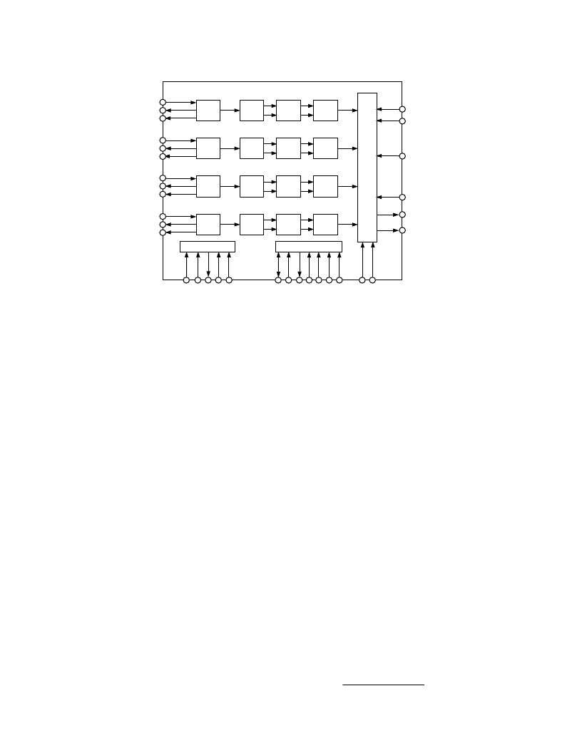
SPORT
SDINA
SDFSA
SCLKA
DATA
RCF
I
Q
CIC
FILTER
I
Q
NCO
DATa
JTAG
T
T
T
T
MICROPORT
D
D
R
W
D
M
A
C
SPORT
SDINB
SDFSB
SCLKB
DATA
RCF
I
Q
CIC
FILTER
I
Q
NCO
DATb
SPORT
SDINC
SDFSC
SCLKC
DATA
RCF
I
Q
CIC
FILTER
I
Q
NCO
DATc
SPORT
SDIND
SDFSD
SCLKD
DATA
RCF
I
Q
CIC
FILTER
I
Q
NCO
DATd
S
C
R
QIN
IN
[17:0]
SYNC
OEN
QOUT
OUT
[17:0]
T
AD6622
Figure 9. Functional Block Diagram
相关PDF资料 |
PDF描述 |
|---|---|
| AD6622S | Four-Channel, 75 MSPS Digital Transmit Signal Processor TSP |
| AD6622 | Four-Channel, 75 MSPS Digital Transmit Signal Processor TSP |
| AD6623 | 4-Channel, 104 MSPS Digital Transmit Signal Processor TSP |
| AD6623ABC | 4-Channel, 104 MSPS Digital Transmit Signal Processor TSP |
| AD6623AS | 4-Channel, 104 MSPS Digital Transmit Signal Processor TSP |
相关代理商/技术参数 |
参数描述 |
|---|---|
| AD6622S | 制造商:AD 制造商全称:Analog Devices 功能描述:Four-Channel, 75 MSPS Digital Transmit Signal Processor TSP |
| AD6622S/PCB | 制造商:AD 制造商全称:Analog Devices 功能描述:Four-Channel, 75 MSPS Digital Transmit Signal Processor TSP |
| AD6623 | 制造商:Analog Devices 功能描述: |
| AD6623ABC | 制造商:Analog Devices 功能描述:Signal Processor 196-Pin CSP-BGA 制造商:Rochester Electronics LLC 功能描述:4 CHANNEL, 104 MSPS DIGITAL TSP - Bulk |
| AD6623ABCZ | 制造商:Analog Devices 功能描述:Signal Processor 196-Pin CSP-BGA |
发布紧急采购,3分钟左右您将得到回复。