- 您现在的位置:买卖IC网 > PDF目录373890 > AD6630AR (ANALOG DEVICES INC) Differential, Low Noise IF Gain Block with Output Clamping PDF资料下载
参数资料
| 型号: | AD6630AR |
| 厂商: | ANALOG DEVICES INC |
| 元件分类: | 消费家电 |
| 英文描述: | Differential, Low Noise IF Gain Block with Output Clamping |
| 中文描述: | SPECIALTY CONSUMER CIRCUIT, PDSO16 |
| 封装: | 0.300 INCH, PLASTIC, SOIC-16 |
| 文件页数: | 3/8页 |
| 文件大小: | 129K |
| 代理商: | AD6630AR |

–3–
REV. 0
AD6630
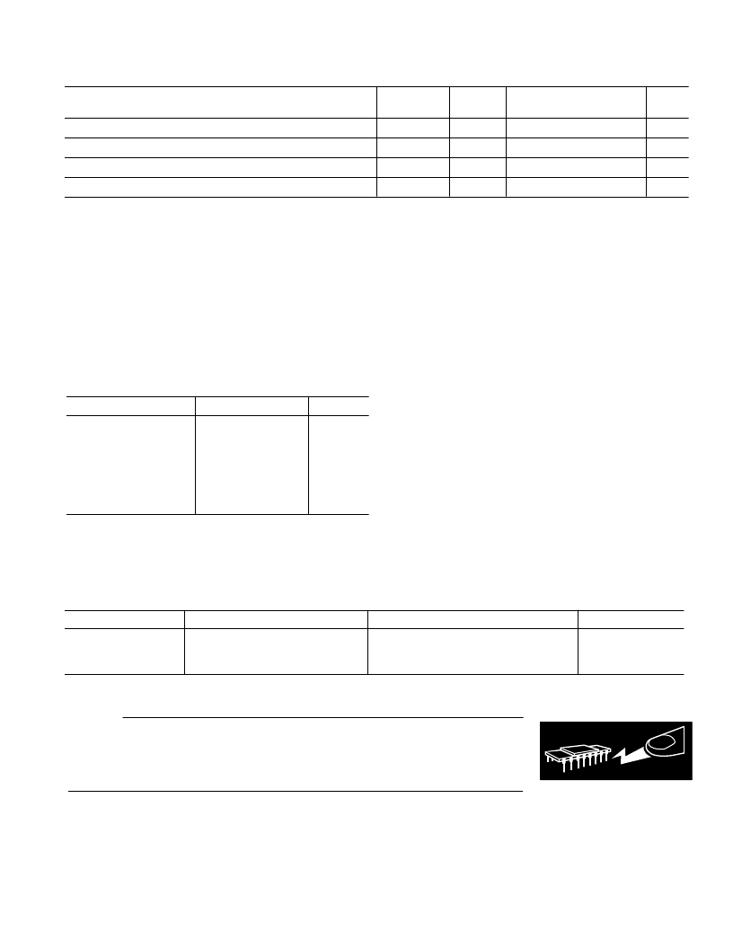
Test
Level
Parameter
HIGH LEVEL CLAMP MAXIMUM OUTPUT @ 250 MHz
4, 5
PHASE VARIATION
6
Temp
Min
Typ
Max
Units
Full
+25
°
C
+25
°
C
+25
°
C
IV
11.2
12.2
dBm
V
9
Degree
CMRR
7
PSRR
8
V
50
dB
V
30
dB
NOTES
1
All specifications are valid across the operating frequency range when the source and load impedance are a conjugate match to the amplifier’s input and output
impedance.
2
Test is for two tones separated by 1 MHz for IFs at 70 MHz and 250 MHz at –23 dBm per tone input.
3
Low Level Clamp is selected by connecting pin CLLO to the negative supply, while pin CLHI is left floating. Clamping can be set at lower levels by connecting pin
CLLO and CLHI to the negative supply through an external resistor.
4
High Level Clamp is selected by connecting pin CLHI to the negative supply, while pin CLLO is left floating, this allows the maximum linear range of the device to
be utilized.
5
Output clamp levels are measured for hard clamping with a +3 dBm input level. Valid for a maximum input level of +8 dBm/200
= 3.2 V p-p—differential.
6
Measured as the change in output phase when the input level is changed from –53 dBm to +8 dBm (i.e., from linear operation to clamping).
7
Ratio of the differential output signal (referenced to the input) to the common-mode input signal presented to all input pins.
8
Ratio of signal on supply to differential output (<500 kHz).
Specifications subject to change without notice.
ABSOLUTE MAXIMUM RATINGS
Parameter
Min
Max
Units
Single Supply Voltage
Positive Supply Voltage
Negative Supply Voltage
Input Power
Storage Temperature
Junction Temperature
ESD Protection
–0.5
–0.5
–5.75
11.5
5.75
0.5
+8
+150
+150
V
V
V
dBm
°
C
°
C
kV
–65
1
EXPLANATION OF TEST LEVELS
I.
100% production tested.
II.
100% production tested at +25
°
C, and guaranteed by
design and analysis at temperature extremes.
III. Sample tested only.
IV. Parameter guaranteed by design and analysis.
V.
Parameter is typical value only.
VI. 100% production tested at +25
°
C, and sample tested at
temperature extremes.
ORDERING GUIDE
Model
Temperature Range
–40
°
C to +85
°
C (Ambient)
–40
°
C to +85
°
C (Ambient)
Package Description
Package Option
AD6630AR
AD6630AR-REEL
AD6630R/PCB
16-Lead Wide Body SOIC
AD6630AR on 1000 PC Reel
Evaluation Board with AD6630AR
R-16
CAUTION
ESD (electrostatic discharge) sensitive device. Electrostatic charges as high as 4000 V readily
accumulate on the human body and test equipment and can discharge without detection.
Although the AD6630 features proprietary ESD protection circuitry, permanent damage may
occur on devices subjected to high energy electrostatic discharges. Therefore, proper ESD
precautions are recommended to avoid performance degradation or loss of functionality.
WARNING!
ESD SENSITIVE DEVICE
相关PDF资料 |
PDF描述 |
|---|---|
| AD6630PCB | Differential, Low Noise IF Gain Block with Output Clamping |
| AD6630R | Differential, Low Noise IF Gain Block with Output Clamping |
| AD6633 | Multichannel Digital Upconverter with VersaCREST Crest Reduction Engine |
| AD6634 | 80 MSPS, Dual-Channel WCDMA Receive Signal Processor (RSP) |
| AD6634BBC | 80 MSPS, Dual-Channel WCDMA Receive Signal Processor (RSP) |
相关代理商/技术参数 |
参数描述 |
|---|---|
| AD6630AR-REEL | 制造商:Rochester Electronics LLC 功能描述:- Tape and Reel |
| AD6630ARZ | 功能描述:IC IF GAIN BLOCK W/CLAMP 16SOIC RoHS:是 类别:RF/IF 和 RFID >> RF 放大器 系列:- 标准包装:3,000 系列:- 频率:100MHz ~ 6GHz P1dB:9.14dBm(8.2mW) 增益:15.7dB 噪音数据:1.3dB RF 型:CDMA,TDMA,PCS 电源电压:2.7 V ~ 5 V 电流 - 电源:60mA 测试频率:2GHz 封装/外壳:0505(1412 公制) 包装:带卷 (TR) |
| AD6630ARZ-REEL | 制造商:Rochester Electronics LLC 功能描述: 制造商:Analog Devices 功能描述: |
| AD6630PCB | 制造商:AD 制造商全称:Analog Devices 功能描述:Differential, Low Noise IF Gain Block with Output Clamping |
| AD6630R | 制造商:AD 制造商全称:Analog Devices 功能描述:Differential, Low Noise IF Gain Block with Output Clamping |
发布紧急采购,3分钟左右您将得到回复。