- 您现在的位置:买卖IC网 > PDF目录373890 > AD6630R (Analog Devices, Inc.) Differential, Low Noise IF Gain Block with Output Clamping PDF资料下载
参数资料
| 型号: | AD6630R |
| 厂商: | Analog Devices, Inc. |
| 英文描述: | Differential, Low Noise IF Gain Block with Output Clamping |
| 中文描述: | 微分,中频增益低噪声块与输出钳位 |
| 文件页数: | 5/8页 |
| 文件大小: | 129K |
| 代理商: | AD6630R |
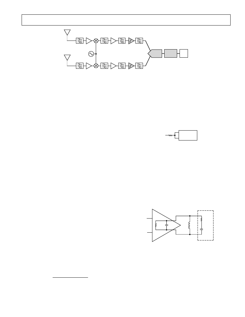
AD6630
–5–
REV. 0
AD6630
DSP
MAIN
DIVERSITY
AD6600
–28dBm
–29dBm
LOCAL
OSCILLATOR
–14dBm
–23dBm
–25dBm
–10dBm
–15dBm
9dBm
4dBm
–1dB
15dB –9dB
–2dB
15dB
–5dB
24dB
–5dB
SAW
SAW
ANTENNA
–104dBm
–43dBm
–28dBm
–16dBm
–15dBm
AD6630 INPUT
–91dBm
–30dBm
–15dBm
–3dBm
–2dBm
AD6630 OUTPUT
–67dBm
–6dBm
+9dBm
+9dBm
+9dBm
AD6600 INPUT
–71dBm
–10dBm
+4dBm
+4dBm
+4dBm
AD6620
Figure 6. GSM Design Example
THEORY OF OPERATION
The AD6630 amplifier consists of two stages of gain. The first
stage is differential. This differential amplifier provides good
common-mode rejection to common-mode signals passed by
the SAW filter. The second stage consists of matched current
feedback amplifiers on each side of the differential pair. These
amplifiers provide additional gain as well as output drive capa-
bility. Gain set resistors for these stages are internal to the de-
vice and cannot be changed, allowing fixed compensation for
optimum performance.
Clamping levels for the device are normally set by tying CLLO
or CLHI pins to the negative supply. This internally sets bias
points that generate symmetric clamping levels. Clamping is
achieved primarily in the output amplifiers. Additional input
stage clamping is provided for additional protection. Clamping
levels may be adjusted to lower levels as discussed below.
APPLICATIONS
The AD6630 provides several useful features to meet the needs
of radio designers. The gain and low noise figure of the device
make it perfect for providing interstage gain between differential
SAW filters and/or analog-to-digital converters (ADC). Addi-
tionally, the on-board clamping circuitry provides protection for
sensitive SAW filters or ADCs. The fast recovery of the clamp
circuit permits demodulation of constant envelope modulated
IF signals by preserving the phase response during clamping.
The following topics provide recommendations for using the
AD6630 in narrowband, single carrier applications.
Adjusting Output Clamp Levels
Normally, the output clamp level is set by tying either CLLO or
CLHI to ground or V
EE
. It is possible to set the limit between
8.5 dBm and 12 dBm levels by selecting the appropriate exter-
nal resistor.
To set to a different level, CLLO and CLHI should be tied
together and then through a resistor to ground. The value of the
resistor can be selected using the following equation.
R
OUTPUT
0 0014
.
dBm
CLAMP
=
14 4
.
–
(
)
This equation is derived from measured data at 170 MHz. Clamp
levels vary with frequency, see Figure 5. Output clamp levels
less than 8.5 dBm will result in damage to the clamp circuitry
unless the absolute maximum input power is derated. Similarly,
the output clamp level cannot be set higher than 12 dBm.
CLAMP
GENERATOR
R
V
EE
Figure 7. Clamp Level Resistor
Matching SAW Filters
The AD6630 is designed to easily match to SAW filters. SAW
filters are largely capacitive in nature. Normally a conjugate
match to the load is desired for maximum power transfer.
Another way to treat the problem is to make the SAW filter look
purely resistive. If the SAW filter load looks resistive there is no
lead or lag in the current vs. voltage. This may not preserve
maximum power transfer, but maximum voltage swing will
exist. All that is required to make the SAW filter input or output
look real is a single inductor shunted across the input. When the
correct value is used, the impedance of the SAW filter becomes
real.
400
V
3pF
47nH
9.7
V
15.2pF
Figure 8. Saw Filter Model (170 MHz)
EVALUATION BOARD
Figures 9, 10 and 12 refer to the schematic and layout of the
AD6630AR as used on Analog Devices’ GSM Diversity Re-
ceiver Reference Design (only the IF section is shown). Figure
14 references the schematic of the stand-alone AD6630 evalua-
tion board and uses a similar layout. The evaluation board uses
center tapped transformers to convert the input to a differential
signal and AD6630 outputs to a single connector to simplify
evaluation. C8, C9 and L2 are optional reactive components to
tune the load for a particular IF frequency if desired.
相关PDF资料 |
PDF描述 |
|---|---|
| AD6633 | Multichannel Digital Upconverter with VersaCREST Crest Reduction Engine |
| AD6634 | 80 MSPS, Dual-Channel WCDMA Receive Signal Processor (RSP) |
| AD6634BBC | 80 MSPS, Dual-Channel WCDMA Receive Signal Processor (RSP) |
| AD6634PCB | 80 MSPS, Dual-Channel WCDMA Receive Signal Processor (RSP) |
| AD6635 | 4-Channel, 80 MSPS WCDMA Receive Signal Processor (RSP) |
相关代理商/技术参数 |
参数描述 |
|---|---|
| AD6630R/PCB | 制造商:AD 制造商全称:Analog Devices 功能描述:Differential, Low Noise IF Gain Block with Output Clamping |
| AD6633 | 制造商:AD 制造商全称:Analog Devices 功能描述:Multichannel Digital Upconverter with VersaCREST Crest Reduction Engine |
| AD6633BBC | 制造商:Rochester Electronics LLC 功能描述: 制造商:Analog Devices 功能描述: |
| AD6633BBCZ | 功能描述:IC DIGITAL UPCONV 6CH 196-CSPBGA RoHS:是 类别:RF/IF 和 RFID >> RF 混频器 系列:AD6633 产品培训模块:Lead (SnPb) Finish for COTS Obsolescence Mitigation Program 标准包装:100 系列:- RF 型:W-CDMA 频率:2.11GHz ~ 2.17GHz 混频器数目:1 增益:17dB 噪音数据:2.2dB 次要属性:- 电流 - 电源:11.7mA 电源电压:2.7 V ~ 3.3 V 包装:托盘 封装/外壳:12-VFQFN 裸露焊盘 供应商设备封装:12-QFN-EP(3x3) |
| AD6633BC/PCB | 制造商:Analog Devices 功能描述:Evaluation Board For Multi-Channel Digital Up-Converter With Versacrest Crest Reduction Engine 制造商:Analog Devices 功能描述:EVALUATION BOARD AD6633 - Bulk 制造商:Rochester Electronics LLC 功能描述:- Bulk |
发布紧急采购,3分钟左右您将得到回复。