- 您现在的位置:买卖IC网 > PDF目录11786 > AD6641BCPZ-500 (Analog Devices Inc)IC IF RCVR 11BIT 200MSPS 56LFCSP PDF资料下载
参数资料
| 型号: | AD6641BCPZ-500 |
| 厂商: | Analog Devices Inc |
| 文件页数: | 16/28页 |
| 文件大小: | 0K |
| 描述: | IC IF RCVR 11BIT 200MSPS 56LFCSP |
| 标准包装: | 1 |
| 应用: | 无线通信系统 |
| 接口: | CMOS,LVDS,并联, 串行,SPI |
| 电源电压: | 1.8 V ~ 2 V |
| 封装/外壳: | 56-VFQFN 裸露焊盘,CSP |
| 供应商设备封装: | 56-LFCSP-VQ(8x8) |
| 包装: | 托盘 |
| 安装类型: | 表面贴装 |
第1页第2页第3页第4页第5页第6页第7页第8页第9页第10页第11页第12页第13页第14页第15页当前第16页第17页第18页第19页第20页第21页第22页第23页第24页第25页第26页第27页第28页
AD6641
Rev. 0 | Page 23 of 28
THEORY OF OPERATION
The on-chip FIFO allows small snapshots of time to be captured
via the ADC and read back at a lower rate. This reduces the
constraints of signal processing by transferring the captured
data at an arbitrary time and at a much lower sample rate.
FIFO OPERATION
The capture of the data can be signaled through writes to the
SPI port by pulsing the FILL± pins. The transaction diagram
shown in Figure 36 illustrates the loading of the FIFO.
At Event 1, the FIFO is instructed to fill either by asserting the
FILL± pins or via a write to the SPI bits. FILL± pin operation
can be delayed by a programmable fill hold-off counter so that
the FIFO data can be surrounding a fill event. The FIFO then
loads itself with data. The number of samples of data is
determined by the SPI fill count register (0x104). This is an 8-
bit register with values from 0 to 255. The number of samples
placed in the FIFO is determined by the following equation:
Number of Samples = (FILL_CNT + 1) × 64
After the FIFO has begun filling at Event 2, the AD6641 asserts
a full flag to indicate that the FIFO has finished capturing data
and enters a wait state in which the device waits to receive the
dump instruction from the DUMP pin or the SPI.
After the data has been shifted (Event 4), the FIFO goes into the
idle state and waits for another fill command. During the idle
state, the ADC can optionally be placed into standby mode to
save power. If the ADC powers down in the idle state, initiating
a fill operation (Event 1) powers up the ADC. In this mode, the
ADC waits for settle count cycles (0x105, 0x106) before capturing
the data. Settle count is programmable from the SPI port and
allows the analog circuitry to stabilize before taking data. An
intelligent trade-off between speed of acquisition and accuracy
can be made by using this register.
The data can be read back through any of the three output inter-
faces at a low data rate, which further saves power. If the SPI or
SPORT is used to read back the data, the interface can require
as few as three pins. A full flag and an empty flag are provided
to signal the state of the FIFO. The FIFO status register (0x10A)
in the SPI also allows this to be monitored via software.
Single Capture Mode
The FIFO can be placed into single capture mode by writing the
FIFO fill mode bits in the fill control register (0x101[3:2]) to 00.
In the single capture mode, the user initiates a capture either by
driving the FILL± pins high or by initiating a fill command
through the SPI port by writing the standby after fill bit
(0x101[0]). This powers up the ADC (if needed) after a
programmable amount of time as determined by the SPI settle
count registers (0x105, 0x106). If Bit 0 of the 0x101 register in
the SPI is set, the ADC returns to standby mode after the
capture is complete.
Fill Pin Timing
A fill of the FIFO can be initiated by asserting the differential
FILL± pins. When a pulse is detected on the FILL± pins, the
FIFO is filled.
Dump Pin Timing
A readback of the FIFO can be initiated by asserting the DUMP
pin. When a logic high is detected on the DUMP pin, the FIFO
data is available through the chosen interface.
09
813
-0
34
1
2
3
4
EVENTS
FILLING FIFO WITH DATA
WAIT FOR DUMP (OPTIONAL)
IDLE STATE
START SP_SCLK AND SP_SDFS SHIFT DATA
IDLE STATE
STATE
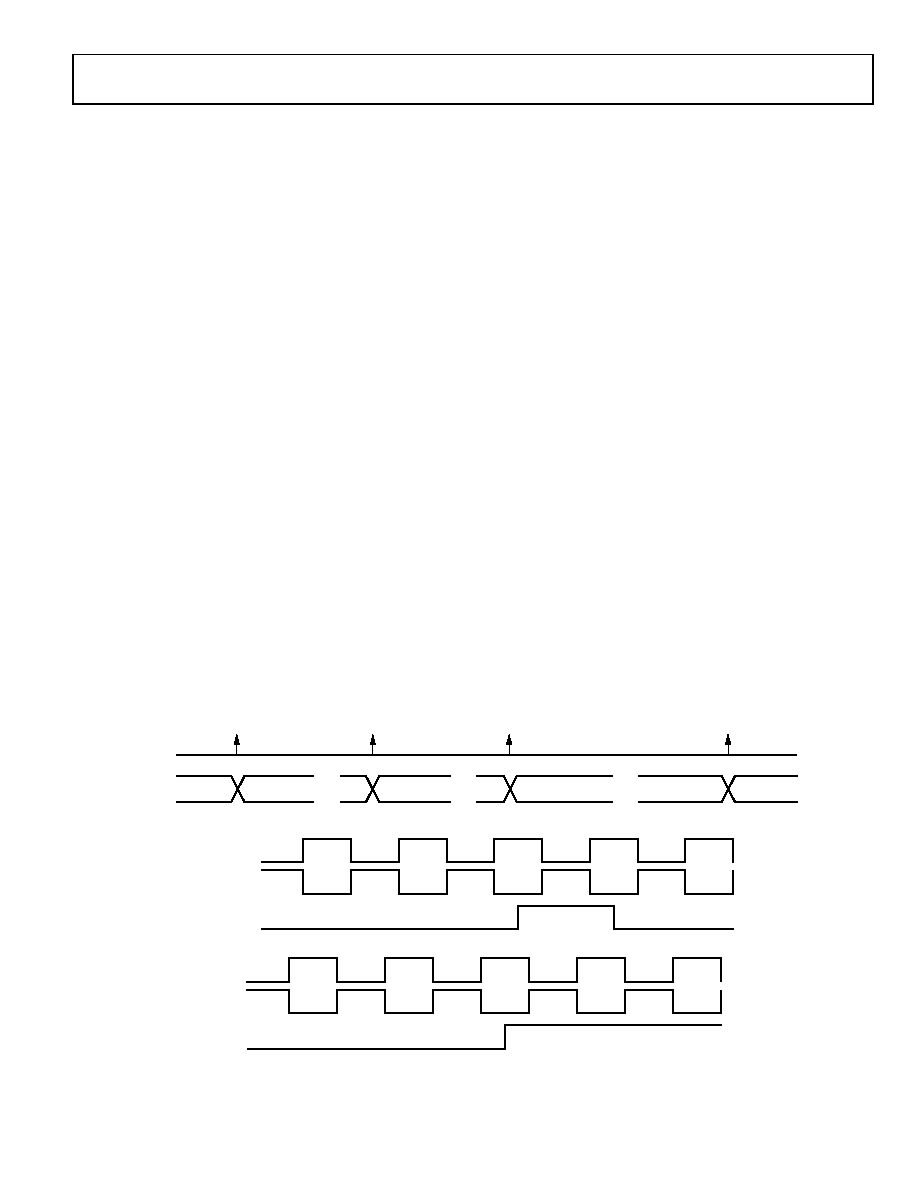
Figure 36. On-Chip FIFO Transaction Timing Assuming Serial Port
CLK+
CLK–
FILL+, FILL–
0
9813-
035
Figure 37. FIFO Fill Timing
0
9813-
036
CLK+
CLK–
DUMP
Figure 38. FIFO DUMP Timing
相关PDF资料 |
PDF描述 |
|---|---|
| VI-JTJ-IW-F3 | CONVERTER MOD DC/DC 36V 100W |
| VI-JTJ-IW-F2 | CONVERTER MOD DC/DC 36V 100W |
| 1604037-4 | CONN HOUSING POWER 2POLE BATTERY |
| VI-JTH-IW-F4 | CONVERTER MOD DC/DC 52V 100W |
| 647845-3 | CONN HOUSING PWR SER 50 2POS RED |
相关代理商/技术参数 |
参数描述 |
|---|---|
| AD6641BCPZRL7-500 | 功能描述:IC IF RCVR 11BIT 200MSPS 56LFCSP RoHS:是 类别:集成电路 (IC) >> 接口 - 专用 系列:- 特色产品:NXP - I2C Interface 标准包装:1 系列:- 应用:2 通道 I²C 多路复用器 接口:I²C,SM 总线 电源电压:2.3 V ~ 5.5 V 封装/外壳:16-TSSOP(0.173",4.40mm 宽) 供应商设备封装:16-TSSOP 包装:剪切带 (CT) 安装类型:表面贴装 产品目录页面:825 (CN2011-ZH PDF) 其它名称:568-1854-1 |
| AD6642 | 制造商:AD 制造商全称:Analog Devices 功能描述:Dual IF Receiver |
| AD6642BBCZ | 功能描述:IC IF RCVR 11BIT 200MSPS 144BGA RoHS:是 类别:RF/IF 和 RFID >> RF 其它 IC 和模块 系列:- 标准包装:100 系列:* |
| AD6642BBCZRL | 功能描述:IC IF RCVR 11BIT 200MSPS 144BGA RoHS:是 类别:RF/IF 和 RFID >> RF 其它 IC 和模块 系列:- 标准包装:100 系列:* |
| AD6642EBZ | 功能描述:BOARD EVALUATION FOR AD6642 RoHS:是 类别:RF/IF 和 RFID >> RF 评估和开发套件,板 系列:- 标准包装:1 系列:- 类型:GPS 接收器 频率:1575MHz 适用于相关产品:- 已供物品:模块 其它名称:SER3796 |
发布紧急采购,3分钟左右您将得到回复。