- 您现在的位置:买卖IC网 > PDF目录10803 > AD664KN-UNI (Analog Devices Inc)IC DAC 12BIT QUAD UNIPOL 28-DIP PDF资料下载
参数资料
| 型号: | AD664KN-UNI |
| 厂商: | Analog Devices Inc |
| 文件页数: | 4/23页 |
| 文件大小: | 0K |
| 描述: | IC DAC 12BIT QUAD UNIPOL 28-DIP |
| 产品培训模块: | Data Converter Fundamentals DAC Architectures |
| 产品变化通告: | Product Discontinuance 27/Oct/2011 |
| 标准包装: | 1 |
| 设置时间: | 8µs |
| 位数: | 12 |
| 数据接口: | 并联 |
| 转换器数目: | 4 |
| 电压电源: | 双 ± |
| 功率耗散(最大): | 525mW |
| 工作温度: | 0°C ~ 70°C |
| 安装类型: | 通孔 |
| 封装/外壳: | 28-DIP(0.600",15.24mm) |
| 供应商设备封装: | 28-PDIP |
| 包装: | 管件 |
| 输出数目和类型: | 4 电压,单极;4 电压,双极 |
| 采样率(每秒): | 125k |
AD664
REV.
–12–
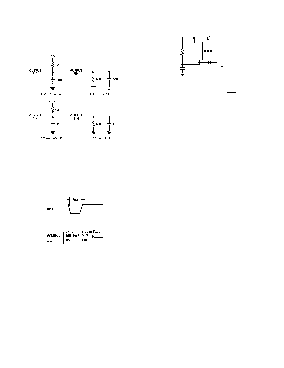
Output Loads
Readback timing is tested with the output loads shown in Figure
22.
Figure 22. Output Loads
Asynchronous Reset Operation
The asynchronous reset signal shown in Figure 23 may be
asserted at any time. A minimum pulse width (tRW) of 90 ns is
required. The reset feature is designed to return all DAC out-
puts to 0 volts regardless of the mode or range selected. In the
44-pin versions, the modes are reset to unipolar 10 V span (gain
of 1), and the input codes are rewritten to be “0s.” Previous
DAC code and mode information is erased.
Figure 23a. Asynchronous Reset Operation
Figure 23b. Asynchronous Reset Operation Timing
In the 28-pin versions of the AD664, the mode remains
unchanged, the appropriate input code is rewritten to reset the
output voltage to 0 volts. As in the 44-pin versions, the previous
input data is erased.
At power-up, an AD664 may be activated in either the read or
write modes. While at the device level this will not produce any
problems, at the system level it may. Analog Devices recom-
mends the addition of a simple power-on reset scheme to any
system where the possibility of an unknown start-up state could
be a problem. The simplest version of this scheme is illustrated
in Figure 24.
AD664
+5V
10k
100nF
#1
RST
#N
RST
Figure 24. Power-On Reset
It is obvious from inspection that the scheme shown in Figure
24 is only appropriate for systems in which the RST is otherwise
not used. Should the user wish to use the RST pin, an addi-
tional logic gate may be included to combine the power-on reset
with the reset signal.
INTERFACING THE AD664 TO MICROPROCESSORS
The AD664 is easy to interface with a wide variety of popular
microprocessors. Common architectures include processors with
dedicated 8-bit data and address buses, an 8-bit bus over which
data and address are multiplexed, an 8-bit data and 16-bit
address partially muxed, and separate 16-bit data and address
buses.
AD664 addressing can be accomplished through either
memory-mapped or I/O techniques. In memory-mapped
schemes, the AD664 appears to the host microprocessor as
RAM memory. Standard memory addressing techniques are
used to select the AD664. In the I/O schemes, the AD664 is
treated as an external I/O device by the host. Dedicated I/O pins
are used to address the AD664.
MC6801 Interface
In Figures 25a–25d, we illustrate a few of the various methods
that can be used to connect an AD664 to the popular MC6801
microprocessor. In each of these cases, the MC6801 is intended
to be configured in its expanded, nonmultiplexed mode of
operation. In this mode, the MC6801 can address 256 bytes of
external memory over 8-bit data (Port 3) and 8-bit address
(Port 4) buses. Eight general-purpose I/O lines (Port 1) are also
available. On-board RAM and ROM provide program and data
storage space.
In Figure 25a, the three least significant address bits (P40, P41
and P42) are employed to select the appropriate on-chip
addresses for the various input registers of the AD664. Three
I/O lines (P17, P16 and P15) are used to select various operat-
ing features of the the AD664. IOS and E(nable) are combined
to produce an appropriate CS signal. This addressing scheme
leaves the five most significant address bits and five I/O lines
free for other tasks in the system.
Figure 25b shows another way to interface an AD664 to the
MC6801. Here we’ve used the six least significant address lines
to select AD664 features and registers. This is a purely memory-
mapped scheme while the one illustrated in Figure 25a uses
some memory-mapping as well as some dedicated I/O pins. In
Figure 25b, two address lines and all eight I/O lines remain free
for other system tasks.
D
相关PDF资料 |
PDF描述 |
|---|---|
| 85106EC145PW50 | CONN PLUG STRAIGHT 5POS W/PIN |
| ADM3078EYRZ | IC TXRX RS-485 3V HD 8SOIC |
| AD5542JR-REEL7 | IC DAC 16BIT SERIAL-IN 14-SOIC |
| ADM206ANZ | IC TXRX RS-232 5V SD/EN 24-DIP |
| AD5542JR | IC DAC 16BIT SERIAL-IN 14-SOIC |
相关代理商/技术参数 |
参数描述 |
|---|---|
| AD664KNZ-BIP | 功能描述:IC DAC 12BIT QUAD BIPOLAR 28DIP RoHS:是 类别:集成电路 (IC) >> 数据采集 - 数模转换器 系列:- 产品培训模块:Lead (SnPb) Finish for COTS Obsolescence Mitigation Program 标准包装:1,000 系列:- 设置时间:1µs 位数:8 数据接口:串行 转换器数目:8 电压电源:双 ± 功率耗散(最大):941mW 工作温度:0°C ~ 70°C 安装类型:表面贴装 封装/外壳:24-SOIC(0.295",7.50mm 宽) 供应商设备封装:24-SOIC W 包装:带卷 (TR) 输出数目和类型:8 电压,单极 采样率(每秒):* |
| AD664KNZ-UNI | 功能描述:IC DAC 12BIT QUAD UNIPOL 28DIP RoHS:是 类别:集成电路 (IC) >> 数据采集 - 数模转换器 系列:- 产品培训模块:Lead (SnPb) Finish for COTS Obsolescence Mitigation Program 标准包装:1,000 系列:- 设置时间:1µs 位数:8 数据接口:串行 转换器数目:8 电压电源:双 ± 功率耗散(最大):941mW 工作温度:0°C ~ 70°C 安装类型:表面贴装 封装/外壳:24-SOIC(0.295",7.50mm 宽) 供应商设备封装:24-SOIC W 包装:带卷 (TR) 输出数目和类型:8 电压,单极 采样率(每秒):* |
| AD664KP | 功能描述:IC DAC 12BIT QUAD MONO 44-PLCC RoHS:否 类别:集成电路 (IC) >> 数据采集 - 数模转换器 系列:- 产品培训模块:Lead (SnPb) Finish for COTS Obsolescence Mitigation Program 标准包装:1,000 系列:- 设置时间:1µs 位数:8 数据接口:串行 转换器数目:8 电压电源:双 ± 功率耗散(最大):941mW 工作温度:0°C ~ 70°C 安装类型:表面贴装 封装/外壳:24-SOIC(0.295",7.50mm 宽) 供应商设备封装:24-SOIC W 包装:带卷 (TR) 输出数目和类型:8 电压,单极 采样率(每秒):* |
| AD664KPZ | 功能描述:IC DAC 12BIT QUAD MONO 44-PLCC RoHS:是 类别:集成电路 (IC) >> 数据采集 - 数模转换器 系列:- 产品培训模块:Lead (SnPb) Finish for COTS Obsolescence Mitigation Program 标准包装:1,000 系列:- 设置时间:1µs 位数:8 数据接口:串行 转换器数目:8 电压电源:双 ± 功率耗散(最大):941mW 工作温度:0°C ~ 70°C 安装类型:表面贴装 封装/外壳:24-SOIC(0.295",7.50mm 宽) 供应商设备封装:24-SOIC W 包装:带卷 (TR) 输出数目和类型:8 电压,单极 采样率(每秒):* |
| AD664SD-BIP | 功能描述:数模转换器- DAC IC QUAD 12-BIT DAC IC RoHS:否 制造商:Texas Instruments 转换器数量:1 DAC 输出端数量:1 转换速率:2 MSPs 分辨率:16 bit 接口类型:QSPI, SPI, Serial (3-Wire, Microwire) 稳定时间:1 us 最大工作温度:+ 85 C 安装风格:SMD/SMT 封装 / 箱体:SOIC-14 封装:Tube |
发布紧急采购,3分钟左右您将得到回复。