参数资料
| 型号: | AD667KP |
| 厂商: | Analog Devices Inc |
| 文件页数: | 7/8页 |
| 文件大小: | 0K |
| 描述: | IC DAC 12BIT W/BUFF LATCH 28PLCC |
| 产品培训模块: | Data Converter Fundamentals DAC Architectures |
| 标准包装: | 1 |
| 设置时间: | 3µs |
| 位数: | 12 |
| 转换器数目: | 1 |
| 电压电源: | 双 ± |
| 功率耗散(最大): | 1W |
| 工作温度: | 0°C ~ 70°C |
| 安装类型: | 表面贴装 |
| 封装/外壳: | 28-LCC(J 形引线) |
| 供应商设备封装: | 28-PLCC(11.51x11.51) |
| 包装: | 管件 |
| 输出数目和类型: | 1 电压,单极;1 电压,双极 |
| 采样率(每秒): | 500k |
AD667
REV. A
–7–
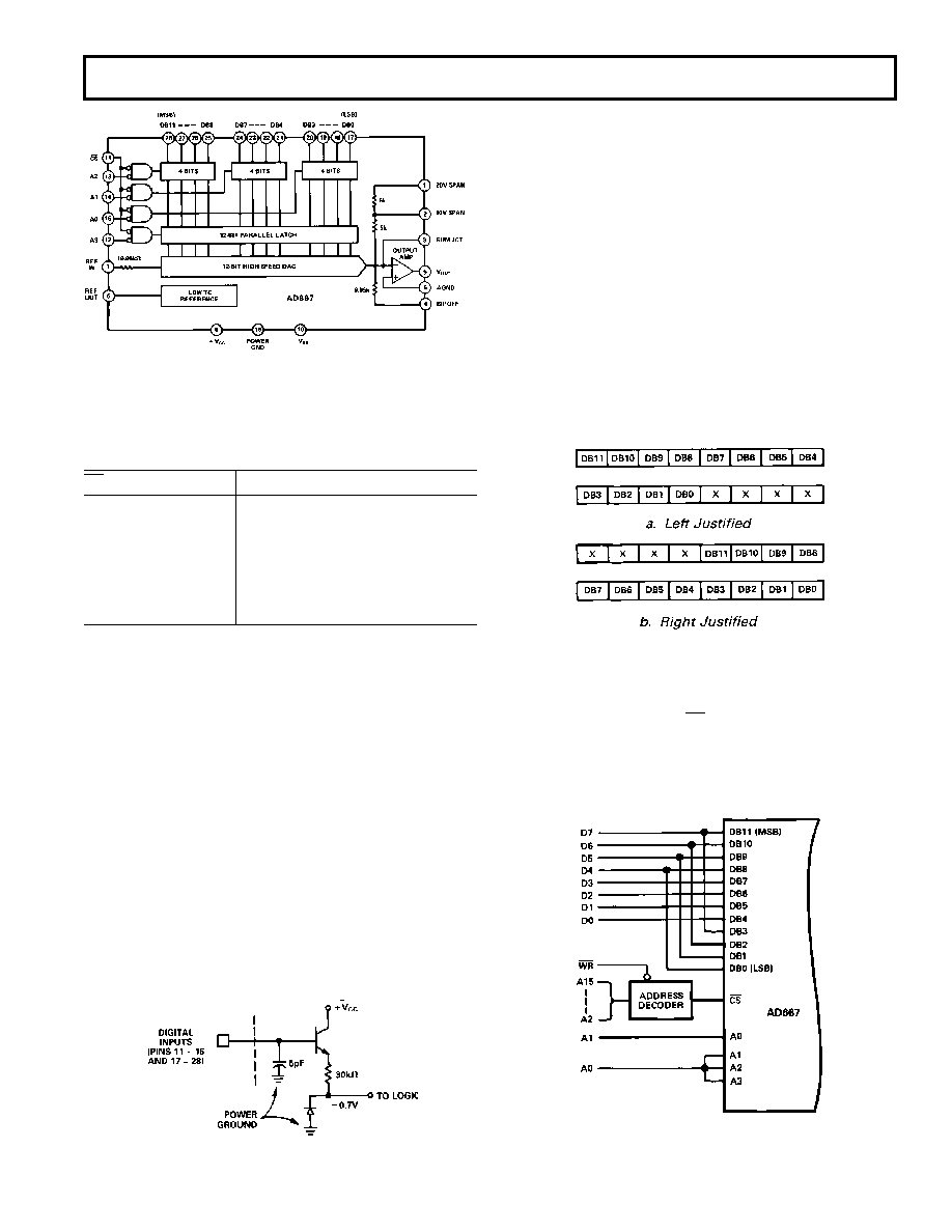
Figure 5. AD667 Block Diagram
It is permissible to enable more than one of the latches simulta-
neously. If a first rank latch is enabled coincident with the sec-
ond rank latch, the data will reach the second rank correctly if
the “WRITE CYCLE #1” timing specifications are met.
Table II. AD667 Truth Table
CS
A3
A2
A1
A0
Operation
1
X
No Operation
X
1111No Operation
0
1110
Enable 4 LSBs of First Rank
0
1101
Enable 4 Middle Bits of First Rank
0
1011
Enable 4 MSBs of First Rank
0
0111
Loads Second Rank from First Rank
0
0000
All Latches Transparent
“X” = Don’t Care.
INPUT CODING
The AD667 uses positive-true binary input coding. Logic “1” is
represented by an input voltage greater than 2.0 V and Logic
“0” is defined as an input voltage less than 0.8 V.
Unipolar coding is straight binary, where all zeroes (000H) on
the data inputs yields a zero analog output and all ones (FFFH)
yields an analog output 1 LSB below full scale.
Bipolar coding is offset binary, where an input code of 000H
yields a minus full-scale output, an input of FFFH yields an out-
put 1 LSB below positive full scale, and zero occurs for an input
code with only the MSB on (800H).
The AD667 can be used with twos complement input coding if
an inverter is used on the MSB (DB11).
DIGITAL INPUT CONSIDERATIONS
The threshold of the digital input circuitry is set at 1.4 volts and
does not vary with supply voltage. The input lines can thus in-
terface with any type of 5 volt logic. The configuration of the in-
put circuit is shown in Figure 6.
Figure 6. Equivalent Digital Input Circuit
The AD667 data and control inputs will float to a Logic 0 if left
open. It is recommended that any unused inputs be connected
to power ground to improve noise immunity.
Fanout for the AD667 is 100 when used with a standard low
power Schottky gate output device.
8-BIT MICROPROCESSOR INTERFACE
The AD667 interfaces easily to 8-bit microprocessor systems of
all types. The control logic makes possible the use of right- or
left-justified data formats.
Whenever a 12-bit DAC is loaded from an 8-bit bus, two bytes
are required. If the program considers the data to be a 12-bit
binary fraction (between 0 and 4095/4096), the data is left-
justified, with the eight most significant bits in one byte and the
remaining bits in the upper half of another byte. Right-justified
data calls for the eight least significant bits to occupy one byte,
with the 4 most significant bits residing in the lower half of an-
other byte, simplifying integer arithmetic.
Figure 7. 12-Bit Data Formats for 8-Bit Systems
Figure 8 shows an addressing scheme for use with an AD667 set
up for left-justified data in an 8-bit system. The base address is
decoded from the high-order address bits and the resultant
active-low signal is applied to CS. The two LSBs of the address
bus are connected as shown to the AD667 address inputs. The
latches now reside in two consecutive locations, with location
X01 loading the four LSBs and location X10 loading the eight
MSBs and updating the output.
Figure 8. Left-Justified 8-Bit Bus Interface
相关PDF资料 |
PDF描述 |
|---|---|
| AD7542KRZ | IC DAC 12BIT MULT CMOS 16SOIC |
| AD7537JP | IC DAC 12BIT DUAL MULT 28-PLCC |
| AD7542KPZ | IC DAC 12BIT MULT CMOS 20PLCC |
| AD667AD | IC DAC 12BIT W/BUFF LTCH 28-CDIP |
| LTC1596ACSW#PBF | IC D/A CONV 16BIT MLTPLYNG16SOIC |
相关代理商/技术参数 |
参数描述 |
|---|---|
| AD667KP-REEL | 制造商:Rochester Electronics LLC 功能描述:- Tape and Reel |
| AD667KPZ | 功能描述:IC DAC 12BIT W/BUFF LATCH 28PLCC RoHS:是 类别:集成电路 (IC) >> 数据采集 - 数模转换器 系列:- 标准包装:1 系列:- 设置时间:4.5µs 位数:12 数据接口:串行,SPI? 转换器数目:1 电压电源:单电源 功率耗散(最大):- 工作温度:-40°C ~ 125°C 安装类型:表面贴装 封装/外壳:8-SOIC(0.154",3.90mm 宽) 供应商设备封装:8-SOICN 包装:剪切带 (CT) 输出数目和类型:1 电压,单极;1 电压,双极 采样率(每秒):* 其它名称:MCP4921T-E/SNCTMCP4921T-E/SNRCTMCP4921T-E/SNRCT-ND |
| AD667KPZ-REEL | 功能描述:IC DAC 12BIT W/BUFF LATCH 28PLCC RoHS:是 类别:集成电路 (IC) >> 数据采集 - 数模转换器 系列:- 产品培训模块:Data Converter Fundamentals DAC Architectures 标准包装:750 系列:- 设置时间:7µs 位数:16 数据接口:并联 转换器数目:1 电压电源:双 ± 功率耗散(最大):100mW 工作温度:0°C ~ 70°C 安装类型:表面贴装 封装/外壳:28-LCC(J 形引线) 供应商设备封装:28-PLCC(11.51x11.51) 包装:带卷 (TR) 输出数目和类型:1 电压,单极;1 电压,双极 采样率(每秒):143k |
| AD667SD | 功能描述:数模转换器- DAC IC - 12-BIT D/A CONVERTER RoHS:否 制造商:Texas Instruments 转换器数量:1 DAC 输出端数量:1 转换速率:2 MSPs 分辨率:16 bit 接口类型:QSPI, SPI, Serial (3-Wire, Microwire) 稳定时间:1 us 最大工作温度:+ 85 C 安装风格:SMD/SMT 封装 / 箱体:SOIC-14 封装:Tube |
| AD667SD/883B | 功能描述:数模转换器- DAC IC - 12-BIT D/A CONVERTER RoHS:否 制造商:Texas Instruments 转换器数量:1 DAC 输出端数量:1 转换速率:2 MSPs 分辨率:16 bit 接口类型:QSPI, SPI, Serial (3-Wire, Microwire) 稳定时间:1 us 最大工作温度:+ 85 C 安装风格:SMD/SMT 封装 / 箱体:SOIC-14 封装:Tube |
发布紧急采购,3分钟左右您将得到回复。