参数资料
| 型号: | AD669BNZ |
| 厂商: | Analog Devices Inc |
| 文件页数: | 2/12页 |
| 文件大小: | 0K |
| 描述: | IC DAC 16BIT MONO W/VREF 28-DIP |
| 产品培训模块: | Data Converter Fundamentals DAC Architectures |
| 产品变化通告: | AD669 Improvement Change 11/Jul/2012 |
| 标准包装: | 13 |
| 系列: | DACPORT® |
| 设置时间: | 10µs |
| 位数: | 16 |
| 数据接口: | 并联 |
| 转换器数目: | 1 |
| 电压电源: | 双 ± |
| 功率耗散(最大): | 625mW |
| 工作温度: | -40°C ~ 85°C |
| 安装类型: | 通孔 |
| 封装/外壳: | 28-DIP(0.600",15.24mm) |
| 供应商设备封装: | 28-PDIP |
| 包装: | 管件 |
| 输出数目和类型: | 1 电压,单极;1 电压,双极 |
| 采样率(每秒): | 167k |
| 产品目录页面: | 781 (CN2011-ZH PDF) |
AD669
REV. A
–10–
tied together which configures the input stage as an edge trig-
gered 16-bit register. The rising edge of the decoded signal
latches the data and updates the output of the DAC. It is neces-
sary to insert wait states after the processor initiates the write
cycle to comply with the timing requirements tLOW shown in
Figure 1b. The number of wait states that are required will vary
depending on the processor cycle time. The equation given in
Figure 9 can be used to determine the number of wait states
given the frequency of the processor crystal.
A0–A15
DSP56001
D0–D23
DGND
+5V
EXTERNAL
CLOCK
ADDRESS
DECODE
74F32
LDAC
AD669
DGND
DB0–DB15
XTAL
CS
L1
DS
X/
Y
WR
IRQA
V
LL
CS1
T =
1
2 (XTAL)
t
– T + 9ns
2T
LOW
# OF
WAIT STATES =
V
LL
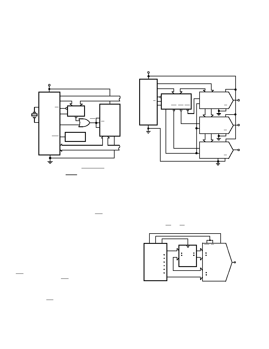
Figure 9. DSP56001 to AD669 Interface
As an example, the 20.48 MHz crystal used in this application
results in T = 24.4 ns which means that the required number of
wait states is about 2.76. This must be rounded to the next
highest integer to assure that the minimum pulse widths comply
with those required by the AD669. As the speed of the proces-
sor is increased, the data hold time relative to CS1 decreases. As
processor clocks increase beyond 20.48 MHz, a configuration
such as the one shown for the ADSP-2101 is the better choice.
AD669 TO 8086 INTERFACE
Figure 10 shows the 8086 16-bit microprocessor connected to
multiple AD669s. The double-buffered capability of the AD669
allows the microprocessor to write to each AD669 individually
and then update all the outputs simultaneously. Processor
speeds of 6, 8, and 10 MHz require no wait states to interface
with the AD669.
The 8086 software routine begins by writing a data word to the
CS1
address. The decoder must latch the address using the
ALE signal. The decoded CS1 pulse goes low causing the first
rank latch of the associated AD669 to become transparent.
Simultaneously, the 8086 places data on the multiplexed bus
which is then latched into the first rank of the AD669 with the
rising edge of the WR pulse. Care should be taken to prevent
excessive delays through the decoder potentially resulting in a
violation of the AD669 data hold time (tDH).
The same procedure is repeated until all three AD669s have had
their first rank latches loaded with the desired data. A final write
command to the LDAC address results in a high-going pulse
that causes the second rank latches of all the AD669s to become
transparent. The falling edge of LDAC latches the data from the
first rank until the next update. This scheme is easily expanded
to include as many AD669s as required.
8086
DGND
+5V
ALE
WR
M/I0
ADDRESS
DECODE
LDAC CS1 CS2 CS3
DGND L1
DB0 – DB15
LDAC
AD669
VOUT
AD0 – AD15
DGND L1
DB0 – DB15
LDAC
AD669
VOUT
DGND L1
DB0 – DB15
LDAC
AD669
CS
VOUT
V
LL
V
LL
V
LL
V
LL
CS
Figure 10. 8086-to-AD669 Interface
8-BIT MICROPROCESSOR INTERFACE
The AD669 can easily be operated with an 8-bit bus by the ad-
dition of an octal latch. The 16-bit first rank register is loaded
from the 8-bit bus as two bytes. Figure 11 shows the configura-
tion when using a 74HC573 octal latch.
The eight most significant bits are latched into the 74HC573 by
setting the “latch enable” control line low. The eight least sig-
nificant bits are then placed onto the bus. Now all sixteen bits
can be simultaneously loaded into the first rank register of the
AD669 by setting CS and L1 low.
8-BIT
P
AND
CONTROL
D7
D0
D7
D0
Q7
Q0
74HC573
11
LDAC
MSB
DB8
DB7
LSB
AD669
CS1 L1
Figure 11. Connections for 8-Bit Bus Interface
相关PDF资料 |
PDF描述 |
|---|---|
| AD7237AQ | IC DAC 12BIT W/AMP W/BUFF 24CDIP |
| VI-26T-IV | CONVERTER MOD DC/DC 6.5V 150W |
| VI-BNP-MU-S | CONVERTER MOD DC/DC 13.8V 200W |
| VI-26M-IV | CONVERTER MOD DC/DC 10V 150W |
| AD5390BSTZ-3 | IC DAC 14BIT 16CHAN 3V 52LQFP |
相关代理商/技术参数 |
参数描述 |
|---|---|
| AD669BQ | 制造商:AD 制造商全称:Analog Devices 功能描述:Monolithic 16-Bit DACPORT |
| AD669BR | 功能描述:IC DAC 16BIT MONO W/VREF 28-SOIC RoHS:否 类别:集成电路 (IC) >> 数据采集 - 数模转换器 系列:DACPORT® 产品培训模块:Lead (SnPb) Finish for COTS Obsolescence Mitigation Program 标准包装:1,000 系列:- 设置时间:1µs 位数:8 数据接口:串行 转换器数目:8 电压电源:双 ± 功率耗散(最大):941mW 工作温度:0°C ~ 70°C 安装类型:表面贴装 封装/外壳:24-SOIC(0.295",7.50mm 宽) 供应商设备封装:24-SOIC W 包装:带卷 (TR) 输出数目和类型:8 电压,单极 采样率(每秒):* |
| AD669BR-REEL | 功能描述:IC DAC 16BIT MONO VREF 28-SOIC RoHS:否 类别:集成电路 (IC) >> 数据采集 - 数模转换器 系列:DACPORT® 产品培训模块:Data Converter Fundamentals DAC Architectures 标准包装:750 系列:- 设置时间:7µs 位数:16 数据接口:并联 转换器数目:1 电压电源:双 ± 功率耗散(最大):100mW 工作温度:0°C ~ 70°C 安装类型:表面贴装 封装/外壳:28-LCC(J 形引线) 供应商设备封装:28-PLCC(11.51x11.51) 包装:带卷 (TR) 输出数目和类型:1 电压,单极;1 电压,双极 采样率(每秒):143k |
| AD669BRZ | 功能描述:IC DAC 16BIT MONO W/VREF 28-SOIC RoHS:是 类别:集成电路 (IC) >> 数据采集 - 数模转换器 系列:DACPORT® 产品培训模块:Lead (SnPb) Finish for COTS Obsolescence Mitigation Program 标准包装:50 系列:- 设置时间:4µs 位数:12 数据接口:串行 转换器数目:2 电压电源:单电源 功率耗散(最大):- 工作温度:-40°C ~ 85°C 安装类型:表面贴装 封装/外壳:8-TSSOP,8-MSOP(0.118",3.00mm 宽) 供应商设备封装:8-uMAX 包装:管件 输出数目和类型:2 电压,单极 采样率(每秒):* 产品目录页面:1398 (CN2011-ZH PDF) |
| AD669BRZ-REEL | 功能描述:IC DAC 16BIT MONO VREF 28-SOIC RoHS:是 类别:集成电路 (IC) >> 数据采集 - 数模转换器 系列:DACPORT® 产品培训模块:Data Converter Fundamentals DAC Architectures 标准包装:750 系列:- 设置时间:7µs 位数:16 数据接口:并联 转换器数目:1 电压电源:双 ± 功率耗散(最大):100mW 工作温度:0°C ~ 70°C 安装类型:表面贴装 封装/外壳:28-LCC(J 形引线) 供应商设备封装:28-PLCC(11.51x11.51) 包装:带卷 (TR) 输出数目和类型:1 电压,单极;1 电压,双极 采样率(每秒):143k |
发布紧急采购,3分钟左右您将得到回复。