- 您现在的位置:买卖IC网 > PDF目录10143 > AD670JPZ (Analog Devices Inc)IC ADC 8BIT SIGNAL COND 20-PLCC PDF资料下载
参数资料
| 型号: | AD670JPZ |
| 厂商: | Analog Devices Inc |
| 文件页数: | 7/12页 |
| 文件大小: | 0K |
| 描述: | IC ADC 8BIT SIGNAL COND 20-PLCC |
| 标准包装: | 1 |
| 位数: | 8 |
| 采样率(每秒): | 10k |
| 数据接口: | 并联 |
| 转换器数目: | 1 |
| 功率耗散(最大): | 450mW |
| 电压电源: | 单电源 |
| 工作温度: | 0°C ~ 70°C |
| 安装类型: | 表面贴装 |
| 封装/外壳: | 20-LCC(J 形引线) |
| 供应商设备封装: | 20-PLCC(9x9) |
| 包装: | 管件 |
| 输入数目和类型: | 1 个差分,单极;1 个差分,双极 |
AD670
REV. A
–4–
ORDERING GUIDE
Temperature
Relative Accuracy
Gain Accuracy
Model
1
Range
@ +25 C
Package Option
2
AD670JN
0
°C to +70°C
±1/2 LSB
±1.5 LSB
Plastic DIP (N-20)
AD670JP
0
°C to +70°C
±1/2 LSB
±1.5 LSB
PLCC (P-20A)
AD670KN
0
°C to +70°C
±1/4 LSB
±0.75 LSB
Plastic DIP (N-20)
AD670KP
0
°C to +70°C
±1/4 LSB
±0.75 LSB
PLCC (P-20A)
AD670AD
–40
°C to +85°C
±1/2 LSB
±1.5 LSB
Ceramic DIP (D-20)
AD670BD
–40
°C to +85°C
±1/4 LSB
±0.75 LSB
Ceramic DIP (D-20)
AD670SD
–55
°C to +125°C
±1/2 LSB
±1.5 LSB
Ceramic DIP (D-20)
NOTES
1For details on grade and package offerings screened in accordance with MIL-STD-883 refer to the Analog Devices
Military Products Databook.
2D = Ceramic DIP; N = Plastic DIP; P = Plastic Leaded Chip Carrier.
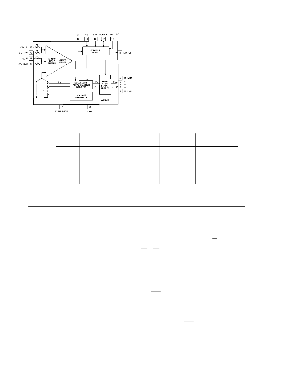
Figure 1. AD670 Block Diagram and Terminal
Configuration (AII Packages)
ABSOLUTE MAXIMUM RATINGS*
VCC to Ground . . . . . . . . . . . . . . . . . . . . . . . . . . . 0 V to +7.5 V
Digital Inputs (Pins 11–15) . . . . . . . . . . . –0.5 V to VCC +0.5 V
Digital Outputs (Pins 1–9) . Momentary Short to VCC or Ground
Analog Inputs (Pins 16–19) . . . . . . . . . . . . . . . –30 V to +30 V
Power Dissipation . . . . . . . . . . . . . . . . . . . . . . . . . . . . 450 mW
Storage Temperature Range . . . . . . . . . . . . . –65
°C to +150°C
Lead Temperature (Soldering, 10 sec) . . . . . . . . . . . . . +300
°C
*Stresses above those listed under “Absolute Maximum Ratings” may cause
permanent damage to the device. This is a stress rating only and functional
operation of the device at them or any other conditions above those indicated in
the operational sections of this specification is not implied. Exposure to absolute
maximum rating conditions for extended periods may affect device reliability.
CIRCUIT OPERATION/FUNCTIONAL DESCRIPTION
The AD670 is a functionally complete 8-bit signal conditioning
A/D converter with microprocessor compatibility. The input
section uses an instrumentation amplifier to accomplish the
voltage to current conversion. This front end provides a high
impedance, low bias current differential amplifier. The com-
mon-mode range allows the user to directly interface the device
to a variety of transducers.
The AID conversions are controlled by R/W, CS, and CE. The
R/W line directs the converter to read or start a conversion. A
minimum write/start pulse of 300 ns is required on either CE or
CS
. The STATUS line goes high, indicating that a conversion is
in process. The conversion thus begun, the internal 8-bit DAC
is sequenced from MSB to LSB using a novel successive ap-
proximation technique. In conventional designs, the DAC is
stepped through the bits by a clock. This can be thought of as a
static design since the speed at which the DAC is sequenced is
determined solely by the clock. No clock is used in the AD670.
Instead, a “dynamic SAR” is created consisting of a string of in-
verters with taps along the delay line. Sections of the delay line
between taps act as one shots. The pulses are used to set and re-
set the DAC’s bits and strobe the comparator. When strobed,
the comparator then determines whether the addition of each
successively weighted bit current causes the DAC current sum
to be greater or less than the input current. If the sum is less,
the bit is turned off. After all bits are tested, the SAR holds an
8-bit code representing the input signal to within 1/2 LSB
accuracy. Ease of implementation and reduced dependence on
process related variables make this an attractive approach to a
successive approximation design.
The SAR provides an end-of-conversion signal to the control
logic which then brings the STATUS line low. Data outputs re-
main in a high impedance state until R/W is brought high with
CE
and CS low and allows the converter to be read. Bringing
CE
or CS high during the valid data period ends the read cycle.
The output buffers cannot be enabled during a conversion. Any
convert start commands will be ignored until the conversion
cycle is completed; once a conversion cycle has been started it
cannot be stopped or restarted.
The AD670 provides the user with a great deal of flexibility by
offering two input spans and formats and a choice of output
codes. Input format and input range can each be selected. The
BPO/UPO pin controls a switch which injects a bipolar offset
current of a value equal to the MSB less 1/2 LSB into the sum-
ming node of the comparator to offset the DAC output. Two
precision 10 to 1 attenuators are included on board to provide
input range selection of 0 V to 2.55 V or 0 mV to 255 mV. Ad-
ditional ranges of –1.28 V to 1.27 V and –128 mV to 127 mV
are possible if the BPO/UPO switch is high when the conversion
is started. Finally, output coding can be chosen using the FOR-
MAT pin when the conversion is started. In the bipolar mode
and with a Logic 1 on FORMAT, the output is in two’s comple-
ment; with a Logic 0, the output is offset binary.
相关PDF资料 |
PDF描述 |
|---|---|
| VI-224-IW-F1 | CONVERTER MOD DC/DC 48V 100W |
| AD7778ASZ | IC ADC 10BIT 8CHAN HS 44-MQFP |
| VI-223-IW-F4 | CONVERTER MOD DC/DC 24V 100W |
| LTC2247IUH#TRPBF | IC ADC 14BIT 40MSPS SAMPL 32-QFN |
| VI-223-IW-F2 | CONVERTER MOD DC/DC 24V 100W |
相关代理商/技术参数 |
参数描述 |
|---|---|
| AD670JPZ-REEL7 | 功能描述:IC ADC 8BIT SIGNAL COND 20-PLCC RoHS:是 类别:集成电路 (IC) >> 数据采集 - 模数转换器 系列:- 标准包装:1,000 系列:- 位数:12 采样率(每秒):300k 数据接口:并联 转换器数目:1 功率耗散(最大):75mW 电压电源:单电源 工作温度:0°C ~ 70°C 安装类型:表面贴装 封装/外壳:24-SOIC(0.295",7.50mm 宽) 供应商设备封装:24-SOIC 包装:带卷 (TR) 输入数目和类型:1 个单端,单极;1 个单端,双极 |
| AD670KN | 制造商:Analog Devices 功能描述:ADC Single SAR 8-bit Parallel 20-Pin PDIP N 制造商:Rochester Electronics LLC 功能描述:IC - 8-BIT A/D CONVERTER - Bulk |
| AD670KNZ | 功能描述:IC ADC 8BIT SGNL COND 20DIP RoHS:是 类别:集成电路 (IC) >> 数据采集 - 模数转换器 系列:- 产品培训模块:Lead (SnPb) Finish for COTS Obsolescence Mitigation Program 标准包装:2,500 系列:- 位数:12 采样率(每秒):3M 数据接口:- 转换器数目:- 功率耗散(最大):- 电压电源:- 工作温度:- 安装类型:表面贴装 封装/外壳:SOT-23-6 供应商设备封装:SOT-23-6 包装:带卷 (TR) 输入数目和类型:- |
| AD670KP | 制造商:Analog Devices 功能描述:ADC Single SAR 8-bit Parallel 20-Pin PLCC |
| AD670KPZ | 功能描述:IC ADC 8BIT SIGNAL COND 20-PLCC RoHS:是 类别:集成电路 (IC) >> 数据采集 - 模数转换器 系列:- 标准包装:1 系列:- 位数:14 采样率(每秒):83k 数据接口:串行,并联 转换器数目:1 功率耗散(最大):95mW 电压电源:双 ± 工作温度:0°C ~ 70°C 安装类型:通孔 封装/外壳:28-DIP(0.600",15.24mm) 供应商设备封装:28-PDIP 包装:管件 输入数目和类型:1 个单端,双极 |
发布紧急采购,3分钟左右您将得到回复。